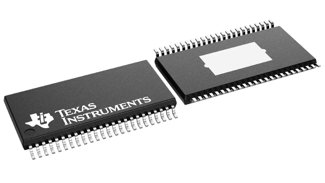
O3850AQDCARQ1
ActiveFUNCTIONAL SAFETY COMPLIANT MULTI-RAIL POWER SUPPLY FOR SAFETY MCUS WITH 350MA I/O RAIL
Deep-Dive with AI
Search across all available documentation for this part.

O3850AQDCARQ1
ActiveFUNCTIONAL SAFETY COMPLIANT MULTI-RAIL POWER SUPPLY FOR SAFETY MCUS WITH 350MA I/O RAIL
Technical Specifications
Parameters and characteristics for this part
| Specification | O3850AQDCARQ1 |
|---|---|
| Current - Supply | 120 mA |
| Grade | Automotive |
| Mounting Type | Surface Mount |
| Operating Temperature [Max] | 125 °C |
| Operating Temperature [Min] | -40 °C |
| Package / Case | 48-PowerTFSOP |
| Package / Case | 0.24 in |
| Package / Case [custom] | 6.1 mm |
| Qualification | AEC-Q100 |
| Supplier Device Package | 48-HTSSOP |
| Voltage - Supply [Max] | 36 V |
| Voltage - Supply [Min] | 7 V |
Pricing
Prices provided here are for design reference only. For realtime values and availability, please visit the distributors directly
| Distributor | Package | Quantity | $ | |
|---|---|---|---|---|
| Digikey | Cut Tape (CT) | 1 | $ 6.87 | |
| 10 | $ 6.20 | |||
| 25 | $ 5.91 | |||
| 100 | $ 5.13 | |||
| 250 | $ 4.90 | |||
| 500 | $ 4.47 | |||
| 1000 | $ 3.89 | |||
| Digi-Reel® | 1 | $ 6.87 | ||
| 10 | $ 6.20 | |||
| 25 | $ 5.91 | |||
| 100 | $ 5.13 | |||
| 250 | $ 4.90 | |||
| 500 | $ 4.47 | |||
| 1000 | $ 3.89 | |||
| Tape & Reel (TR) | 2000 | $ 3.75 | ||
| Texas Instruments | LARGE T&R | 1 | $ 5.25 | |
| 100 | $ 4.28 | |||
| 250 | $ 3.37 | |||
| 1000 | $ 2.86 | |||
Description
General part information
TPS653850A-Q1 Series
The TPS653850A-Q1 and TPS653852A-Q1 device is a multirail power supply designed to supply microcontrollers in safety relevant applications, such as those found in the automotive industry. The device supports functional safety microcontrollers with dual-core lockstep (LS) and other multi-core architectures.
The TPS653850A-Q1 and TPS653852A-Q1 device integrates multiple supply rails to power the MCU, CAN or FlexRay, and external sensors. A buck-boost converter with internal FETs converts the input battery voltage between 2.3 V and 36 V to a 6-V preregulator output that supplies the other regulators. An integrated charge pump provides an overdrive voltage for the internal regulators, and can also be used to drive an external NMOS FET as reverse battery protection. The device supports wake-up from an ignition signal (IGN pin) or wake-up from a CAN transceiver or other signal (CAN_WU pin).
An independent voltage monitoring unit inside the device monitors undervoltage and overvoltage on all internal supply rails and regulator outputs of the battery supply. Regulator current limits and temperature protections are also implemented. The TPS653850A-Q1 and TPS653852A-Q1 device features a question-answer watchdog, MCU error-signal monitor, clock monitoring on internal oscillator, self-check on clock monitor, cyclic redundancy check (CRC) on non-volatile memory and SPI communication, a diagnostic output pin allowing MCU to observe device internal analog and digital signals, a reset circuit for the MCU (NRES pin) and a safing output (ENDRV pin) to disable external power-stages on any detected system-failure. The device automatically runs a built-in self-test (BIST) at start up and the MCU may re-run the BIST during system run time through software control if needed. A dedicated DIAGNOSTIC state allows the MCU to check TPS653850A-Q1 and TPS653852A-Q1 functionality.
Documents
Technical documentation and resources


