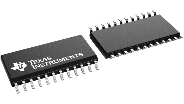
TLC1551IDW
Active10-BIT, 164 KSPS ADC PARALLEL OUT, DIRECT I/F TO DSP/UPROCESSOR, 10 CH.
Deep-Dive with AI
Search across all available documentation for this part.

TLC1551IDW
Active10-BIT, 164 KSPS ADC PARALLEL OUT, DIRECT I/F TO DSP/UPROCESSOR, 10 CH.
Deep-Dive with AI
Technical Specifications
Parameters and characteristics for this part
| Specification | TLC1551IDW |
|---|---|
| Architecture | SAR |
| Configuration | S/H-ADC |
| Data Interface | Parallel |
| Input Type | Single Ended |
| Mounting Type | Surface Mount |
| Number of A/D Converters | 1 |
| Number of Bits [custom] | 10 |
| Number of Inputs | 1 |
| Operating Temperature [Max] | 85 °C |
| Operating Temperature [Min] | -40 °C |
| Package / Case | 24-SOIC |
| Package / Case [custom] | 7.5 mm |
| Package / Case [custom] | 0.295 in |
| Ratio - S/H:ADC | 1:1 |
| Reference Type | External |
| Sampling Rate (Per Second) | 164k |
| Supplier Device Package | 24-SOIC |
| Voltage - Supply, Analog | 5 V |
| Voltage - Supply, Digital | 5 V |
Pricing
Prices provided here are for design reference only. For realtime values and availability, please visit the distributors directly
| Distributor | Package | Quantity | $ | |
|---|---|---|---|---|
| Digikey | Tube | 100 | $ 11.25 | |
| Texas Instruments | TUBE | 1 | $ 11.59 | |
| 100 | $ 10.13 | |||
| 250 | $ 7.81 | |||
| 1000 | $ 6.98 | |||
Description
General part information
TLC1551 Series
The TLC1550x and TLC1551 are data acquisition analog-to-digital converters (ADCs) using a 10-bit, switched-capacitor, successive-approximation network. A high-speed, 3-state parallel port directly interfaces to a digital signal processor (DSP) or microprocessor (µP) system data bus. D0 through D9 are the digital output terminals with D0 being the least significant bit (LSB). Separate power terminals for the analog and digital portions minimize noise pickup in the supply leads. Additionally, the digital power is divided into two parts to separate the lower current logic from the higher current bus drivers. An external clock can be applied to CLKIN to override the internal system clock if desired.
The TLC1550I and TLC1551I are characterized for operation from –40°C to 85°C. The TLC1550M is characterized over the full military range of –55°C to 125°C.
The TLC1550x and TLC1551 are data acquisition analog-to-digital converters (ADCs) using a 10-bit, switched-capacitor, successive-approximation network. A high-speed, 3-state parallel port directly interfaces to a digital signal processor (DSP) or microprocessor (µP) system data bus. D0 through D9 are the digital output terminals with D0 being the least significant bit (LSB). Separate power terminals for the analog and digital portions minimize noise pickup in the supply leads. Additionally, the digital power is divided into two parts to separate the lower current logic from the higher current bus drivers. An external clock can be applied to CLKIN to override the internal system clock if desired.
Documents
Technical documentation and resources


