MPC962305EF-1H
Obsolete1:5 LVCMOS ZERO DELAY BUFFER
Deep-Dive with AI
Search across all available documentation for this part.

MPC962305EF-1H
Obsolete1:5 LVCMOS ZERO DELAY BUFFER
Deep-Dive with AI
Technical Specifications
Parameters and characteristics for this part
| Specification | MPC962305EF-1H |
|---|---|
| Differential - Input:Output | False |
| Divider/Multiplier | False |
| Frequency - Max [Max] | 133.33 MHz |
| Input | LVCMOS |
| Mounting Type | Surface Mount |
| Number of Circuits | 1 |
| Operating Temperature [Max] | 85 °C |
| Operating Temperature [Min] | -40 °C |
| Output | LVCMOS |
| Package / Case | 8-SOIC |
| Package / Case [x] | 0.154 in |
| Package / Case [y] | 3.9 mm |
| PLL | True |
| Ratio - Input:Output | 1:5 |
| Supplier Device Package | 8-SOIC |
| Type | Zero Delay Buffer, Fanout Buffer (Distribution) |
| Voltage - Supply [Max] | 3.6 V |
| Voltage - Supply [Min] | 3 V |
Pricing
Prices provided here are for design reference only. For realtime values and availability, please visit the distributors directly
| Distributor | Package | Quantity | $ | |
|---|---|---|---|---|
Description
General part information
MPC962305 Series
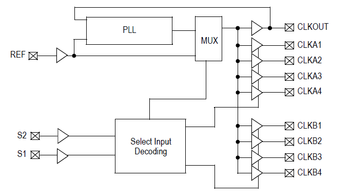
The MPC962309 has two banks of four outputs each, which can be controlled by the Select Inputs as shown in Table 3. Bank B can be tri-stated if all of the outputs are not required. Select inputs also allow the input clock to be directly applied to the outputs for chip and system testing purposes. The MPC962305 and MPC962309 PLLs enters a power down state when there are no rising edges on the REF input. During this state, all of the outputs are in tristate, the PLL is turned off, and there is less than 25.0 ?A of current draw for the device. The PLL shuts down in one additional case as shown in Table 3. Multiple MPC962305 and MPC962309 devices can accept the same input clock and distribute it throughout the system. In this situation, the difference between the output skews of two devices will be less than 700 ps. All outputs have less than 200 ps of cycle-cycle jitter. The input-to-output propagation delay on both devices is guaranteed to be less than 350 ps and the output-to-output skew is guaranteed to be less than 250 ps. The MPC962305 and MPC962309 are available in two/three different configurations, as shown on the ordering information page. The MPC962305-1/MPC962309-1 are the base parts. High drive versions of those devices, MPC962305-1H and MPC962309-1H, are available to provide faster rise and fall times of the base device.
Documents
Technical documentation and resources


