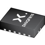
74AXP4T245BQX
ActiveVOLTAGE LEVEL TRANSLATOR CMOS TO CMOS 4-CH BIDIRECTIONAL 16-PIN DHVQFN EP T/R
Deep-Dive with AI
Search across all available documentation for this part.

74AXP4T245BQX
ActiveVOLTAGE LEVEL TRANSLATOR CMOS TO CMOS 4-CH BIDIRECTIONAL 16-PIN DHVQFN EP T/R
Deep-Dive with AI
Technical Specifications
Parameters and characteristics for this part
| Specification | 74AXP4T245BQX |
|---|---|
| Current - Output High, Low [custom] | 12 mA |
| Current - Output High, Low [custom] | 12 mA |
| Logic Type | Translation Transceiver |
| Mounting Type | Surface Mount |
| Number of Bits per Element | 2 |
| Number of Elements | 2 |
| Operating Temperature [Max] | 125 °C |
| Operating Temperature [Min] | -40 °C |
| Output Type | 3-State |
| Package / Case | 16-VFQFN Exposed Pad |
| Supplier Device Package | 16-DHVQFN (2.5x3.5) |
| Voltage - Supply [Max] | 5.5 V |
| Voltage - Supply [Min] | 0.9 V |
Pricing
Prices provided here are for design reference only. For realtime values and availability, please visit the distributors directly
| Distributor | Package | Quantity | $ | |
|---|---|---|---|---|
| Digikey | N/A | 0 | $ 0.96 | |
Description
General part information
74AXP4T245BQ Series
The 74AXP4T245 is an 4-bit dual supply translating transceiver with 3-state outputs that enable bidirectional level translation. The device can be used as two 2-bit transceivers or as a 4-bit transceiver. It features four 2-bit input-output ports (nAn and nBn), a direction control input (nDIR), a output enable input (nOE) and dual supply pins (VCC(A)and VCC(B)). Both VCC(A)and VCC(B)can be supplied at any voltage between 0.9 V and 5.5 V making the device suitable for translating between any of the low voltage nodes (0.9 V, 1.2 V, 1.5 V, 1.8 V, 2.5 V, 3.3 V and 5.0 V). No power supply sequencing is required and output glitches during power supply transitions are prevented using patented circuitry. As a result glitches will not appear on the outputs for supply transitions during power-up/down between 20 mV/µs and 5.5 V/s.
Documents
Technical documentation and resources


