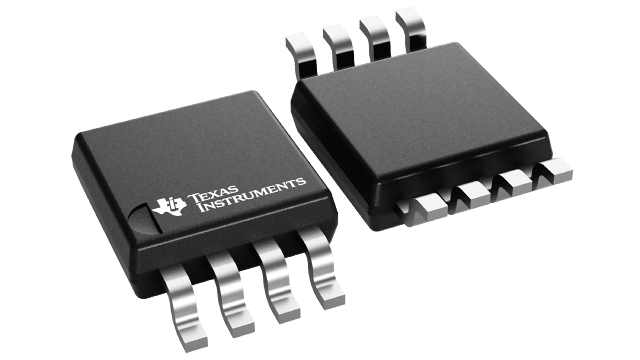
LMH6505MM/NOPB
ActiveSP AMP VARIABLE GAIN AMP SINGLE R-R I/O ±6V/12V 8-PIN VSSOP T/R
Deep-Dive with AI
Search across all available documentation for this part.

LMH6505MM/NOPB
ActiveSP AMP VARIABLE GAIN AMP SINGLE R-R I/O ±6V/12V 8-PIN VSSOP T/R
Deep-Dive with AI
Technical Specifications
Parameters and characteristics for this part
| Specification | LMH6505MM/NOPB |
|---|---|
| -3db Bandwidth | 150 MHz |
| Current - Input Bias | 600 nA |
| Current - Output / Channel | 80 mA |
| Current - Supply | 11 mA |
| Mounting Type | Surface Mount |
| Number of Circuits | 1 |
| Operating Temperature [Max] | 85 °C |
| Operating Temperature [Min] | -40 °C |
| Package / Case | 8-MSOP, 8-TSSOP |
| Package / Case | 3 mm |
| Package / Case [custom] | 0.118 in |
| Slew Rate | 1500 V/µs |
| Voltage - Supply Span (Max) [Max] | 12 V |
| Voltage - Supply Span (Min) [Min] | 7 V |
Pricing
Prices provided here are for design reference only. For realtime values and availability, please visit the distributors directly
| Distributor | Package | Quantity | $ | |
|---|---|---|---|---|
| Digikey | Cut Tape (CT) | 1 | $ 6.12 | |
| 10 | $ 5.53 | |||
| 25 | $ 5.27 | |||
| 100 | $ 4.58 | |||
| 250 | $ 4.37 | |||
| 500 | $ 3.99 | |||
| Digi-Reel® | 1 | $ 6.12 | ||
| 10 | $ 5.53 | |||
| 25 | $ 5.27 | |||
| 100 | $ 4.58 | |||
| 250 | $ 4.37 | |||
| 500 | $ 3.99 | |||
| Tape & Reel (TR) | 1000 | $ 3.47 | ||
| 2000 | $ 3.34 | |||
| Texas Instruments | SMALL T&R | 1 | $ 4.69 | |
| 100 | $ 3.82 | |||
| 250 | $ 3.00 | |||
| 1000 | $ 2.55 | |||
Description
General part information
LMH6505 Series
The LMH6505 is a wideband DC coupled voltage controlled gain stage followed by a high speed current feedback operational amplifier which can directly drive a low impedance load. The gain adjustment range is 80 dB for up to 10 MHz which is accomplished by varying the gain control input voltage, VG.
Maximum gain is set by external components, and the gain can be reduced all the way to cutoff. Power consumption is 110 mW with a speed of 150 MHz and a gain control bandwidth (BW) of 100 MHz. Output referred DC offset voltage is less than 55 mV over the entire gain control voltage range. Device-to-device gain matching is within ±0.5 dB at maximum gain. Furthermore, gain is tested and ensured over a wide range. The output current feedback op amp allows high frequency large signals (Slew Rate = 1500 V/μs) and can also drive a heavy load current (60 mA) ensured.
Near ideal input characteristics (i.e. low input bias current, low offset, low pin 3 resistance) enable the device to be easily configured as an inverting amplifier as well.
Documents
Technical documentation and resources


