Deep-Dive with AI
Search across all available documentation for this part.

Deep-Dive with AI
Technical Specifications
Parameters and characteristics for this part
| Specification | 74VHCT14AN |
|---|---|
| Current - Output High, Low [custom] | 8 mA |
| Current - Output High, Low [custom] | 8 mA |
| Features | Schmitt Trigger |
| Input Logic Level - High [Max] | 2.1 V |
| Input Logic Level - High [Min] | 1.9 V |
| Input Logic Level - Low [Max] | 0.6 V |
| Input Logic Level - Low [Min] | 0.5 V |
| Logic Type | Inverter |
| Max Propagation Delay @ V, Max CL | 9.6 ns |
| Mounting Type | Through Hole |
| Number of Circuits | 6 |
| Number of Inputs | 1 |
| Operating Temperature [Max] | 85 °C |
| Operating Temperature [Min] | -40 °C |
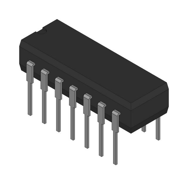
| Package / Case | 14-DIP |
| Package / Case [x] | 0.3 " |
| Package / Case [y] | 7.62 mm |
| Supplier Device Package | 14-DIP |
| Voltage - Supply [Max] | 5.5 V |
| Voltage - Supply [Min] | 4.5 V |
Pricing
Prices provided here are for design reference only. For realtime values and availability, please visit the distributors directly
| Distributor | Package | Quantity | $ | |
|---|---|---|---|---|
| Digikey | Tube | 2427 | $ 0.12 | |
| 2959 | $ 0.10 | |||
Description
General part information
MC74VHCT14A Series
The MC74VHCT14A is an advanced high speed CMOS Schmitt inverter fabricated with silicon gate CMOS technology. It achieves high speed operation similar to equivalent Bipolar Schottky TTL while maintaining CMOS low power dissipation.Pin configuration and function are the same as the MC74VHCT04A, but the inputs have hysteresis and, with its Schmitt trigger function, the VHCT14A can be used as a line receiver which will receive slow input signals.The VHCT inputs are compatible with TTL levels. This device can be used as a level converter for interfacing 3.3V to 5.0V, because it has full 5V CMOS level output swings.The VHCT14A input structures provide protection when voltages between 0V and 5.5V are applied, regardless of the supply voltage.The output structures also provide protection when VCC= 0V. These input and output structures help prevent device destruction caused by supply voltage input/output voltage mismatch, battery backup, hot insertion, etc.The internal circuit is composed of three stages, including a buffer output which provides high noise immunity and stable output. The inputs tolerate voltages up to 7V, allowing the interface of 5V systems to 3V systems.
Documents
Technical documentation and resources
No documents available


