Deep-Dive with AI
Search across all available documentation for this part.

Deep-Dive with AI
Technical Specifications
Parameters and characteristics for this part
| Specification | CDCVF857DGGR |
|---|---|
| Differential - Input:Output [custom] | True |
| Differential - Input:Output [custom] | True |
| Divider/Multiplier | False |
| Frequency - Max [Max] | 220 MHz |
| Input | SSTL-2 |
| Mounting Type | Surface Mount |
| Number of Circuits | 1 |
| Operating Temperature [Max] | 85 °C |
| Operating Temperature [Min] | -40 °C |
| Output | SSTL-2 |
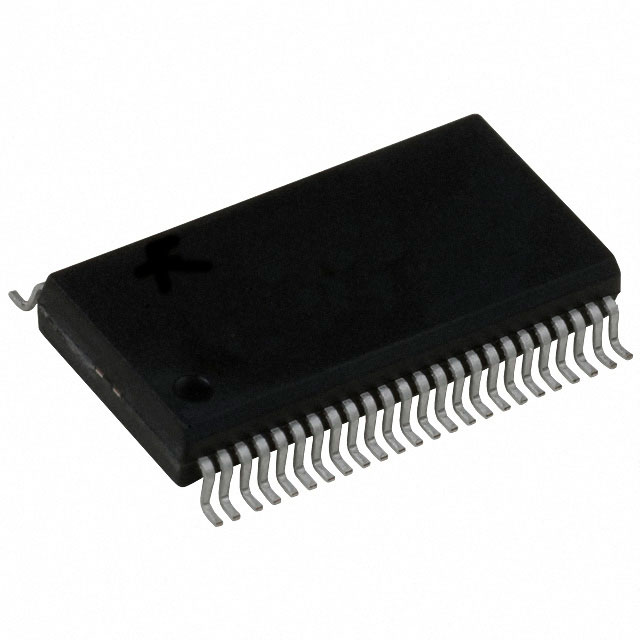
| Package / Case | 48-TFSOP |
| Package / Case | 0.24 in |
| Package / Case [custom] | 6.1 mm |
| PLL | Yes with Bypass |
| Ratio - Input:Output [custom] | 2:11 |
| Supplier Device Package | 48-TSSOP |
| Type | PLL Clock Driver |
| Voltage - Supply [Max] | 2.7 V |
| Voltage - Supply [Min] | 2.3 V |
Pricing
Prices provided here are for design reference only. For realtime values and availability, please visit the distributors directly
| Distributor | Package | Quantity | $ | |
|---|---|---|---|---|
| Digikey | Tape & Reel (TR) | 2000 | $ 4.91 | |
| Texas Instruments | LARGE T&R | 1 | $ 6.88 | |
| 100 | $ 5.61 | |||
| 250 | $ 4.41 | |||
| 1000 | $ 3.74 | |||
Description
General part information
CDCVF857 Series
The CDCVF857 is a high-performance, low-skew, low-jitter, zero-delay buffer that distributes a differential clock input pair (CLK,CLK) to 10 differential pairs of clock outputs (Y[0:9],Y[0:9]) and one differential pair of feedback clock outputs (FBOUT,FBOUT). The clock outputs are controlled by the clock inputs (CLK,CLK), the feedback clocks (FBIN,FBIN), and the analog power input (AVDD). WhenPWRDWNis high, the outputs switch in phase and frequency with CLK. WhenPWRDWNis low, all outputs are disabled to a high-impedance state (3-state) and the PLL is shut down (low-power mode). The device also enters this low-power mode when the input frequency falls below a suggested detection frequency that is below 20 MHz (typical 10 MHz). An input frequency detection circuit detects the low frequency condition and, after applying a >20-MHz input signal, this detection circuit turns the PLL on and enables the outputs.
When AVDDis strapped low, the PLL is turned off and bypassed for test purposes. The CDCVF857 is also able to track spread spectrum clocking for reduced EMI.
Because the CDCVF857 is based on PLL circuitry, it requires a stabilization time to achieve phase-lock of the PLL. This stabilization time is required following power up. The CDCVF857 is characterized for both commercial and industrial temperature ranges.
Documents
Technical documentation and resources


