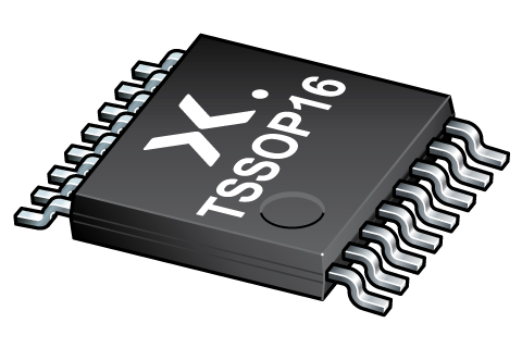
74AVC4T245PW-Q100J
Active4-BIT DUAL SUPPLY TRANSLATING TRANSCEIVER WITH CONFIGURABLE VOLTAGE TRANSLATION; 3-STATE
Deep-Dive with AI
Search across all available documentation for this part.

74AVC4T245PW-Q100J
Active4-BIT DUAL SUPPLY TRANSLATING TRANSCEIVER WITH CONFIGURABLE VOLTAGE TRANSLATION; 3-STATE
Technical Specifications
Parameters and characteristics for this part
| Specification | 74AVC4T245PW-Q100J |
|---|---|
| Current - Output High, Low [custom] | 12 mA |
| Current - Output High, Low [custom] | 12 mA |
| Grade | Automotive |
| Logic Type | Translation Transceiver |
| Mounting Type | Surface Mount |
| Number of Bits per Element | 2 |
| Number of Elements | 2 |
| Operating Temperature [Max] | 125 °C |
| Operating Temperature [Min] | -40 °C |
| Output Type | 3-State |
| Package / Case | 16-TSSOP |
| Package / Case [y] | 4.4 mm |
| Package / Case [y] | 0.173 in |
| Qualification | AEC-Q100 |
| Supplier Device Package | 16-TSSOP |
| Voltage - Supply [Max] | 3.6 V |
| Voltage - Supply [Min] | 0.8 V |
Pricing
Prices provided here are for design reference only. For realtime values and availability, please visit the distributors directly
| Distributor | Package | Quantity | $ | |
|---|---|---|---|---|
| Digikey | N/A | 999 | $ 1.16 | |
Description
General part information
74AVC4T245PW-Q100 Series
The 74AVC4T245-Q100 is an 4-bit, dual supply transceiver that enables bidirectional level translation. The device can be used as two 2-bit transceivers or as a 4-bit transceiver. It features four 2-bit input-output ports (nAn and nBn), a direction control input (nDIR), an output enable input (nOE) and dual supply pins (VCC(A)and VCC(B)). Both VCC(A)and VCC(B)can be supplied at any voltage between 0.8 V and 3.6 V making the device suitable for translating between any of the low voltage nodes (0.8 V, 1.2 V, 1.5 V, 1.8 V, 2.5 V and 3.3 V). Pins nAn, nOEand nDIR are referenced to VCC(A)and pins nBn are referenced to VCC(B). A HIGH on nDIR allows transmission from nAn to nBn and a LOW on nDIR allows transmission from nBn to nAn. The output enable input (nOE) can be used to disable the outputs so the buses are effectively isolated. The device is fully specified for partial power-down applications using IOFF. The IOFFcircuitry disables the output, preventing any damaging backflow current through the device when it is powered down. In suspend mode when either VCC(A)or VCC(B)are at GND level, both nAn and nBn are in the high-impedance OFF-state.
Documents
Technical documentation and resources


