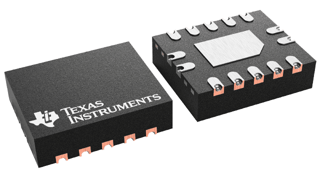
CLV8T164QWBQARQ1
ActiveAUTOMOTIVE, 1.65-V TO 5.5-V 8-BIT, PARALLEL-OUT SERIAL SHIFT REGISTERS WITH LOGIC LEVEL SHIFTER
Deep-Dive with AI
Search across all available documentation for this part.

CLV8T164QWBQARQ1
ActiveAUTOMOTIVE, 1.65-V TO 5.5-V 8-BIT, PARALLEL-OUT SERIAL SHIFT REGISTERS WITH LOGIC LEVEL SHIFTER
Deep-Dive with AI
Technical Specifications
Parameters and characteristics for this part
| Specification | CLV8T164QWBQARQ1 |
|---|---|
| null | |
Pricing
Prices provided here are for design reference only. For realtime values and availability, please visit the distributors directly
| Distributor | Package | Quantity | $ | |
|---|---|---|---|---|
| Texas Instruments | LARGE T&R | 1 | $ 0.66 | |
| 100 | $ 0.51 | |||
| 250 | $ 0.37 | |||
| 1000 | $ 0.27 | |||
Description
General part information
SN74LV8T164-Q1 Series
The SN74LV8T164-Q1 device contains an 8-bit shift register with AND-gated serial inputs and an asynchronous clear (CLR) input. The gated serial (A and B) inputs permit complete control over incoming data; a low at either input inhibits entry of the new data and resets the first flip-flop to the low level at the next clock (CLK) pulse. A high-level input enables the other input, which then determines the state of the first flip-flop. Data at the serial inputs can be changed while CLK is high or low, provided the minimum set-up time requirements are met. Clocking occurs on the low-to-high-level transition of CLK.
The input is designed with a reduced threshold circuit to support up translation when the supply voltage is larger than the input voltage. Additionally, the 5V tolerant input pins enable down translation when the input voltage is larger than the supply voltage. The output level is always referenced to the supply voltage (VCC) and supports 1.8V, 2.5V, 3.3V, and 5V CMOS levels.
The SN74LV8T164-Q1 device contains an 8-bit shift register with AND-gated serial inputs and an asynchronous clear (CLR) input. The gated serial (A and B) inputs permit complete control over incoming data; a low at either input inhibits entry of the new data and resets the first flip-flop to the low level at the next clock (CLK) pulse. A high-level input enables the other input, which then determines the state of the first flip-flop. Data at the serial inputs can be changed while CLK is high or low, provided the minimum set-up time requirements are met. Clocking occurs on the low-to-high-level transition of CLK.
Documents
Technical documentation and resources


