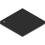
LTC6950IUHH#TRPBF
UnknownCLOCK GENERATOR 2MHZ TO 250MHZ-IN 1400MHZ-OUT 48-PIN QFN EP T/R
Deep-Dive with AI
Search across all available documentation for this part.

LTC6950IUHH#TRPBF
UnknownCLOCK GENERATOR 2MHZ TO 250MHZ-IN 1400MHZ-OUT 48-PIN QFN EP T/R
Deep-Dive with AI
Technical Specifications
Parameters and characteristics for this part
| Specification | LTC6950IUHH#TRPBF |
|---|---|
| Differential - Input:Output | True |
| Divider/Multiplier | Yes/No |
| Frequency - Max [Max] | 1.4 GHz |
| Input | Clock |
| Mounting Type | Surface Mount |
| Number of Circuits | 1 |
| Operating Temperature [Max] | 105 ░C |
| Operating Temperature [Min] | -40 C |
| Output | PECL, CMOS, LVDS |
| Package / Case | 48-WFQFN Exposed Pad |
| PLL | True |
| Ratio - Input:Output | 1:5 |
| Supplier Device Package | 48-QFN |
| Supplier Device Package [x] | 5 mm |
| Supplier Device Package [y] | 9 mm |
| Type | Clock/Frequency Synthesizer, Fanout Buffer (Distribution) |
| Voltage - Supply [Max] | 5.25 V |
| Voltage - Supply [Min] | 3.15 V |
Pricing
Prices provided here are for design reference only. For realtime values and availability, please visit the distributors directly
| Distributor | Package | Quantity | $ | Updated |
|---|---|---|---|---|
| Digikey | N/A | 0 | $ 0.00 | 1m+ |
Description
General part information
LTC6950 Series
The LTC6950 is a low phase noise integer-N frequency synthesizer core with clock distribution. The LTC6950 delivers the low phase noise clock signals demanded in high frequency, high resolution data acquisition systems.The frequency synthesizer contains a full low noise PLL core with a programmable reference divider (R), a programmable feedback divider (N), a phase/frequency detector (PFD) and a low noise charge pump (CP). The clock distribution section of the LTC6950 delivers up to five outputs based on the VCO input. Each output is individually programmed to divide the VCO input frequency by any integer from 1 to 63 and to delay the output by 0 to 63 VCO clock cycles. Four of the outputs feature very low noise, low skew LVPECL logic signals capable of operation up to 1.4GHz. The fifth output is selectable as either an LVDS (800MHz) or CMOS (250MHz) logic type. This output is also programmed to produce an output signal based on either the VCO input or the reference divider output.ApplicationsClocking High Speed, High Resolution ADCs, DACs and Data Acquisition SystemsLow Jitter Clock Generation and Distribution
Documents
Technical documentation and resources


