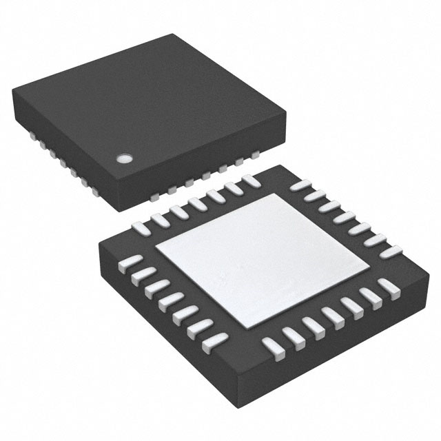
TPS6565342RHDRQ1
ActiveAUTOMOTIVE 4-MHZ, DUAL 3-A BUCK CONVERTERS WITH INTEGRATED SWITCHES
Deep-Dive with AI
Search across all available documentation for this part.

TPS6565342RHDRQ1
ActiveAUTOMOTIVE 4-MHZ, DUAL 3-A BUCK CONVERTERS WITH INTEGRATED SWITCHES
Technical Specifications
Parameters and characteristics for this part
| Specification | TPS6565342RHDRQ1 |
|---|---|
| Grade | Automotive |
| Mounting Type | Surface Mount |
| Number of Outputs | 2 |
| Operating Temperature [Max] | 125 °C |
| Operating Temperature [Min] | -40 °C |
| Package / Case | 28-VFQFN Exposed Pad |
| Qualification | AEC-Q100 |
| Supplier Device Package | 28-VQFN (5x5) |
| Voltage - Input [Max] | 5.5 V |
| Voltage - Input [Min] | 2.8 V |
| Voltage - Output [Max] | 3.36 V |
| Voltage - Output [Min] | 1 VDC |
Pricing
Prices provided here are for design reference only. For realtime values and availability, please visit the distributors directly
| Distributor | Package | Quantity | $ | |
|---|---|---|---|---|
| Digikey | N/A | 0 | $ 2.62 | |
| Tape & Reel (TR) | 3000 | $ 2.61 | ||
| Texas Instruments | LARGE T&R | 1 | $ 3.92 | |
| 100 | $ 3.43 | |||
| 250 | $ 2.41 | |||
| 1000 | $ 1.94 | |||
Description
General part information
TPS65653-Q1 Series
The TPS65653-Q1 is designed to provide a tight power specification for noise sensitive applications, such as radar. The device contains two step-down DC/DC converters and general-purpose digital-output signals. The device is controlled by an I2C-compatible serial interface and by an enable signal.
The automatic PWM/PFM (AUTO mode) operation gives high efficiency over a wide output-current range. The TPS65653-Q1 supports remote voltage sensing to compensate IR drop between the regulator output and the point-of-load (POL) thus improving the accuracy of the output voltage. In addition the switching clock can be forced to PWM mode and also synchronized to an external clock to minimize the disturbances.
The TPS65653-Q1 device supports programmable start-up and shutdown delays and sequences including GPO signals synchronized to the enable signal. During start-up and voltage change, the device controls the output slew rate to minimize output voltage overshoot and the in-rush current.


