Deep-Dive with AI
Search across all available documentation for this part.

Deep-Dive with AI
Technical Specifications
Parameters and characteristics for this part
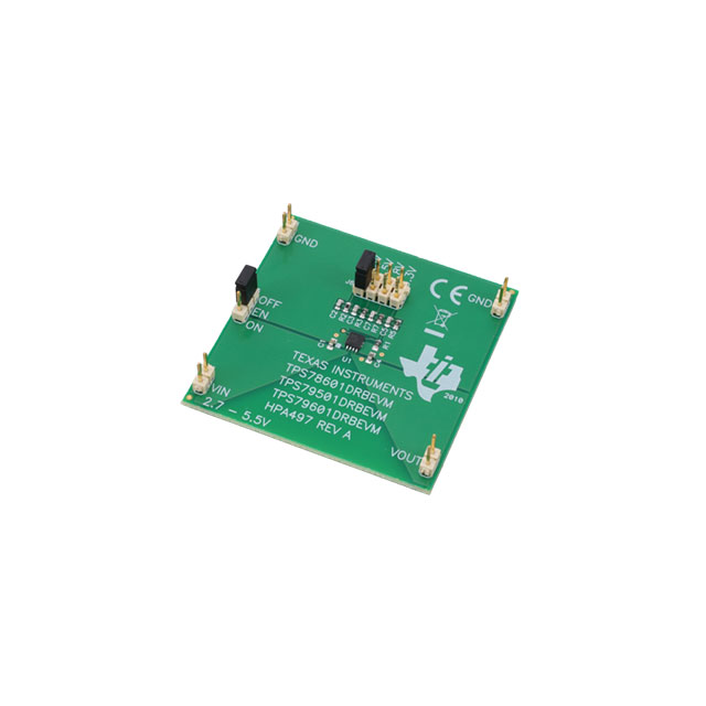
| Specification | TPS79501DRBEVM |
|---|---|
| Board Type | Fully Populated |
| Channels per IC | 1 |
| Contents | Board(s) |
| Current - Output | 500 mA |
| Regulator Type | Positive Adjustable |
| Supplied Contents | Board(s) |
| Utilized IC / Part | TPS79501 |
| Voltage - Input [Max] | 5.5 V |
| Voltage - Input [Min] | 2.7 V |
| Voltage - Output | 2.8 V, 1.8 V, 2.5 V, 3.3 V |
Pricing
Prices provided here are for design reference only. For realtime values and availability, please visit the distributors directly
| Distributor | Package | Quantity | $ | |
|---|---|---|---|---|
| Digikey | Box | 1 | $ 21.12 | |
| N/A | 3 | $ 23.04 | ||
Description
General part information
TPS79501 Series
The TPS79501-Q1 low-dropout (LDO), low-power linear voltage regulator features high power-supply rejection ratio (PSRR), ultralow noise, fast start-up, and excellent line and load transient responses in a small outline SON package. The device is stable with a small 1-µF ceramic capacitor on the output. The TPS79501-Q1 uses an advanced, proprietary BiCMOS fabrication process to yield extremely low dropout voltages (for example, 110 mV at 500 mA). The device achieves fast start-up times (approximately 50 µs with a 0.001-µF bypass capacitor) while consuming very low quiescent current (265 µA, typical). Moreover, when the device is placed in standby mode, the supply current is reduced to less than 1 µA. The TPS79501-Q1 exhibits approximately 33 µVRMSof output voltage noise at 3-V output with a 0.1-µF bypass capacitor. Applications with analog components that are noise-sensitive, such as portable RF electronics, benefit from the high-PSRR and low-noise features, as well as from the fast response time.
The TPS79501-Q1 low-dropout (LDO), low-power linear voltage regulator features high power-supply rejection ratio (PSRR), ultralow noise, fast start-up, and excellent line and load transient responses in a small outline SON package. The device is stable with a small 1-µF ceramic capacitor on the output. The TPS79501-Q1 uses an advanced, proprietary BiCMOS fabrication process to yield extremely low dropout voltages (for example, 110 mV at 500 mA). The device achieves fast start-up times (approximately 50 µs with a 0.001-µF bypass capacitor) while consuming very low quiescent current (265 µA, typical). Moreover, when the device is placed in standby mode, the supply current is reduced to less than 1 µA. The TPS79501-Q1 exhibits approximately 33 µVRMSof output voltage noise at 3-V output with a 0.1-µF bypass capacitor. Applications with analog components that are noise-sensitive, such as portable RF electronics, benefit from the high-PSRR and low-noise features, as well as from the fast response time.
Documents
Technical documentation and resources


