Deep-Dive with AI
Search across all available documentation for this part.

Deep-Dive with AI
Technical Specifications
Parameters and characteristics for this part
| Specification | CD4517BF3A |
|---|---|
| Logic Type | Shift Register |
| Mounting Type | Through Hole |
| Number of Bits per Element | 64 |
| Number of Elements | 2 |
| Operating Temperature [Max] | 125 °C |
| Operating Temperature [Min] | -55 °C |
| Output Type | Tri-State |
| Package / Case | 7.62 mm, 0.3 in |
| Package / Case | 16-CDIP |
| Supplier Device Package | 16-CDIP |
| Voltage - Supply [Max] | 18 V |
| Voltage - Supply [Min] | 3 V |
Pricing
Prices provided here are for design reference only. For realtime values and availability, please visit the distributors directly
| Distributor | Package | Quantity | $ | |
|---|---|---|---|---|
| Texas Instruments | TUBE | 1 | $ 24.54 | |
| 100 | $ 21.43 | |||
| 250 | $ 16.53 | |||
| 1000 | $ 14.78 | |||
Description
General part information
CD4517B-MIL Series
CD4517B dual 64-stage static shift register consists of two independent registers each having a clock, data, and write enable input and outputs accessible at taps following the 16th, 32nd, 48th, and 64th stages. These taps also serve as input points allowing data to be inputted at the 17th, 33rd, and 49th stages when the write enable input is a logic 1 and the clock goes through a low-to-high transition. The truth table indicates how the clock and write enable inputs control the operation of the CD4517B. Inputs at the intermediate taps allow entry of 64 bits into the register with 16 clock pulses. The 3-state outputs permit connection of this device to an external bus.
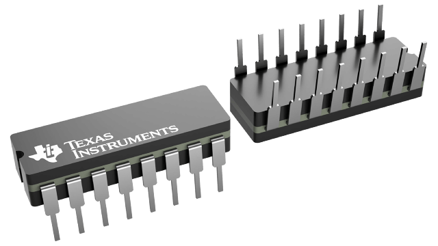
The CD4517B is supplied in 16-lead hermetic dual-in-line ceramic packages (D and F suffixes), 16-lead dual-in-line plastic packages (E suffix), and in chip form (H suffix).
CD4517B dual 64-stage static shift register consists of two independent registers each having a clock, data, and write enable input and outputs accessible at taps following the 16th, 32nd, 48th, and 64th stages. These taps also serve as input points allowing data to be inputted at the 17th, 33rd, and 49th stages when the write enable input is a logic 1 and the clock goes through a low-to-high transition. The truth table indicates how the clock and write enable inputs control the operation of the CD4517B. Inputs at the intermediate taps allow entry of 64 bits into the register with 16 clock pulses. The 3-state outputs permit connection of this device to an external bus.
Documents
Technical documentation and resources


