Zenode.ai Logo
Beta
ROHM SSTA28T116
Discrete Semiconductor Products

SSTA28T116

Active
Rohm Semiconductor

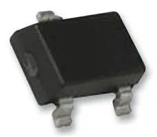
DARLINGTON TRANSISTOR, NPN, 3 PINS

Deep-Dive with AI

Search across all available documentation for this part.

ROHM SSTA28T116
Discrete Semiconductor Products

SSTA28T116

Active
Rohm Semiconductor

DARLINGTON TRANSISTOR, NPN, 3 PINS

Technical Specifications

Parameters and characteristics for this part

SpecificationSSTA28T116
Current - Collector (Ic) (Max) [Max]300 mA
Current - Collector Cutoff (Max) [Max]500 nA
DC Current Gain (hFE) (Min) @ Ic, Vce [Min]10000
Frequency - Transition200 MHz
Mounting TypeSurface Mount
Operating Temperature150 °C
Package / CaseSOT-23-3, TO-236-3, SC-59
Power - Max [Max]200 mW
Supplier Device PackageSST3
Vce Saturation (Max) @ Ib, Ic1.5 V
Voltage - Collector Emitter Breakdown (Max) [Max]80 V

Pricing

Prices provided here are for design reference only. For realtime values and availability, please visit the distributors directly

DistributorPackageQuantity$
DigikeyN/A 3825$ 0.61
NewarkEach (Supplied on Cut Tape) 1$ 0.62
10$ 0.39
25$ 0.32
50$ 0.25
100$ 0.19
250$ 0.18
500$ 0.14
1000$ 0.11

Description

General part information

SSTA28 Series

SSTA28 is bipolar transistor for audio frequency small signal amplifier.

Documents

Technical documentation and resources

Technical Data Sheet EN

Datasheet

Product Change Notice EN

Datasheet

What is a Thermal Model? (Transistor)

Thermal Design

Certificate of not containing SVHC under REACH Regulation

Environmental Data

Taping Information

Package Information

Overview of ROHM's Simulation Models(for ICs and Discrete Semiconductors)

Technical Article

Condition of Soldering / Land Pattern Reference

Package Information

List of Transistor Package Thermal Resistance

Thermal Design

How to Create Symbols for PSpice Models

Models

Impedance Characteristics of Bypass Capacitor

Schematic Design & Verification

Moisture Sensitivity Level - Transistors

Package Information

Method for Monitoring Switching Waveform

Schematic Design & Verification

Calculation of Power Dissipation in Switching Circuit

Schematic Design & Verification

PCB Layout Thermal Design Guide

Thermal Design

Package Dimensions

Package Information

Temperature derating method for Safe Operating Area (SOA)

Schematic Design & Verification

About Flammability of Materials

Environmental Data

Two-Resistor Model for Thermal Simulation

Thermal Design

Importance of Probe Calibration When Measuring Power: Deskew

Schematic Design & Verification

ESD Data

Characteristics Data

How to Use LTspice® Models

Schematic Design & Verification

Reliability Test Result

Manufacturing Data

What Is Thermal Design

Thermal Design

Notes for Temperature Measurement Using Thermocouples

Thermal Design

Compliance of the RoHS directive

Environmental Data

Method for Calculating Junction Temperature from Transient Thermal Resistance Data

Thermal Design

How to Use LTspice® Models: Tips for Improving Convergence

Schematic Design & Verification

About Export Regulations

Export Information

Notes for Calculating Power Consumption:Static Operation

Thermal Design

Notes for Temperature Measurement Using Forward Voltage of PN Junction

Thermal Design

Part Explanation

Application Note

Explanation for Marking

Package Information

Constitution Materials List

Environmental Data

Basics of Thermal Resistance and Heat Dissipation

Thermal Design

Measurement Method and Usage of Thermal Resistance RthJC

Thermal Design

Precautions When Measuring the Rear of the Package with a Thermocouple

Thermal Design

Types and Features of Transistors

Application Note

Anti-Whisker formation - Transistors

Package Information

Inner Structure

Package Information