Deep-Dive with AI
Search across all available documentation for this part.

Deep-Dive with AI
Technical Specifications
Parameters and characteristics for this part
| Specification | FTL11639UCX |
|---|---|
| Current - Output (Max) [Max] | 4.5 A |
| Features | Slew Rate Controlled, Load Discharge |
| Input Type | Non-Inverting |
| Interface | On/Off |
| Mounting Type | Surface Mount |
| Number of Outputs | 1 |
| Operating Temperature [Max] | 85 °C |
| Operating Temperature [Min] | -40 °C |
| Output Configuration | High Side |
| Output Type | P-Channel |
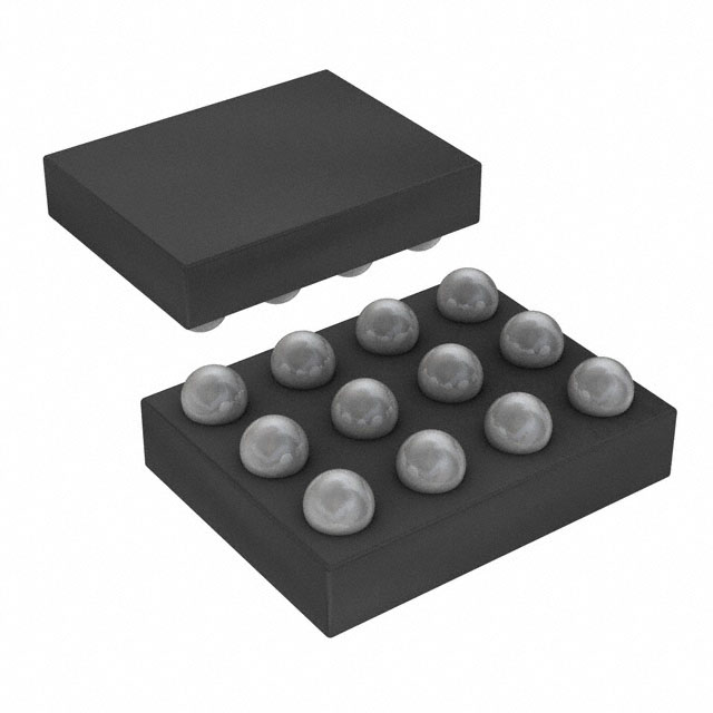
| Package / Case | 12-UFBGA, WLCSP |
| Ratio - Input:Output [custom] | 1:1 |
| Rds On (Typ) | 21 mOhm |
| Supplier Device Package | 12-WLCSP (1.16x1.56) |
| Switch Type | General Purpose |
| Voltage - Supply (Vcc/Vdd) | False |
Pricing
Prices provided here are for design reference only. For realtime values and availability, please visit the distributors directly
| Distributor | Package | Quantity | $ | |
|---|---|---|---|---|
| Digikey | Cut Tape (CT) | 1 | $ 1.00 | |
| Digi-Reel® | 1 | $ 1.00 | ||
Description
General part information
FTL11639 Series
The FTL11639 is both a timer for resetting a mobile device and an advanced load management device for applications requiring a highly integrated solution.If the mobile device is off, holding /SR0 LOW (by pressing power-on key) for 38 ms ±20% turns on the PMIC.As a reset timer, it has one input and one fixed delay output. It generates a fixed delay of 11.5 s ±20% by disconnecting the PMIC from the battery power supply. FTL11639 does not accept a new input signal for 400 ms ±20% to give the PMIC enough time to turn off.The reset delay can be customized by connecting an external resistor to the DELAY_ADJ pin.As an advanced load management switch, the FTL11639 disconnects loads powered from the DC power rail (<6 V) with stringent off-state current targets and high load capacitances (up to 200 µF). The FTL11639 consists of a slew-rate controlled low-impedance MOSFET switch (21 mΏ typical at 4.5 V) that has exceptionally low off-state current drain (<0.2 µA typical) to facilitate compliance with standby power requirements. The slew-rate-controlled turn-on characteristic prevents inrush current and the resulting excessive voltage drop on power rails.The low ICCTenables direct interface to lower-voltage chipsets without external translation, while maintaining low power consumption.The device is packaged in advanced, fully "green," 1.31 mm x 1.62 mm, Wafer-Level Chip-Scale Packaging (WLCSP); providing excellent thermal conductivity, small footprint, and low electrical resistance for a wide application range.
Documents
Technical documentation and resources


