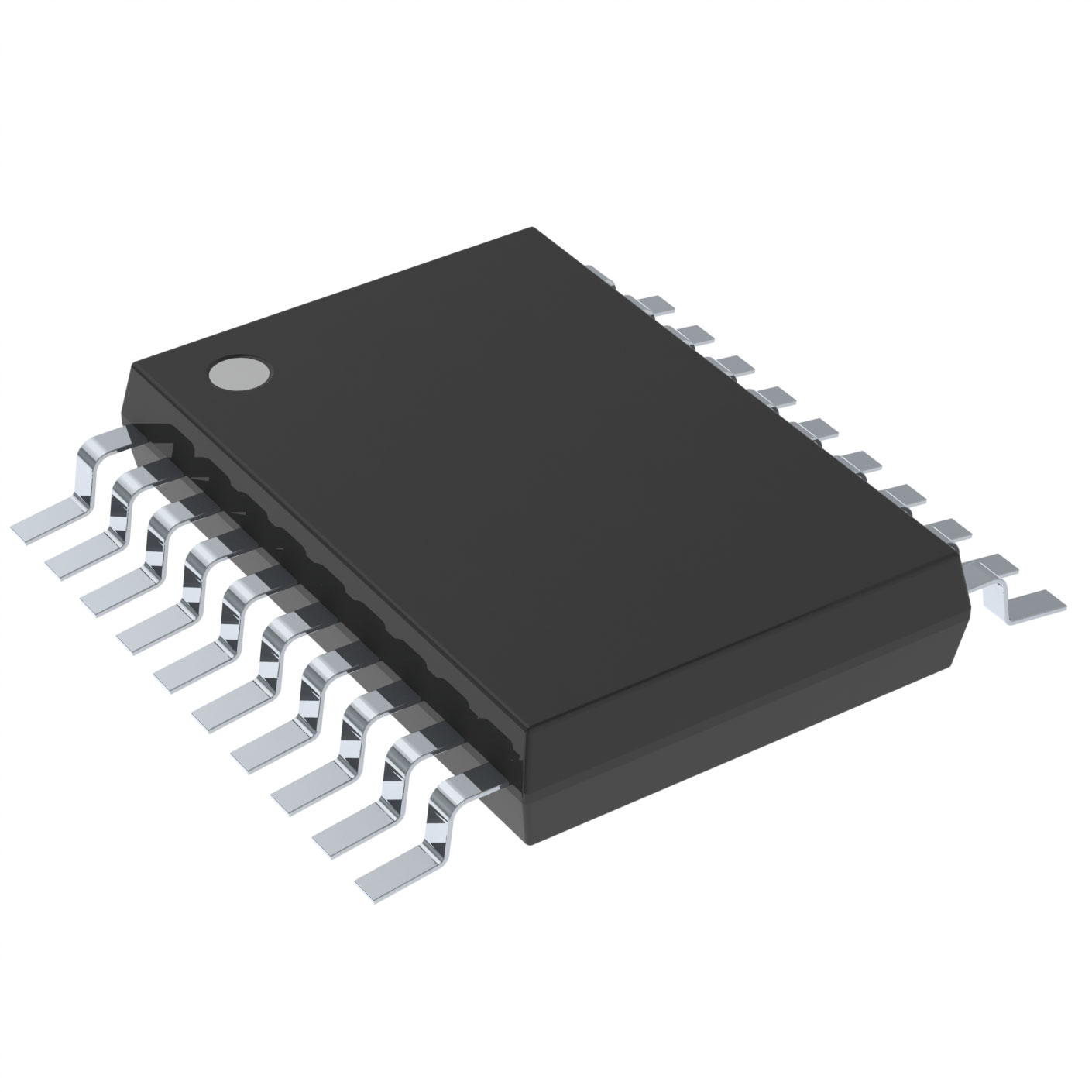
SN74TVC3010DWR
Obsolete6.5-V, 1:1 (SPST), 10-CHANNEL VOLTAGE CLAMP
Deep-Dive with AI
Search across all available documentation for this part.

SN74TVC3010DWR
Obsolete6.5-V, 1:1 (SPST), 10-CHANNEL VOLTAGE CLAMP
Deep-Dive with AI
Technical Specifications
Parameters and characteristics for this part
| Specification | SN74TVC3010DWR |
|---|---|
| Logic Type | Voltage Clamp |
| Mounting Type | Surface Mount |
| Number of Bits [custom] | 10 |
| Operating Temperature [Max] | 85 °C |
| Operating Temperature [Min] | -40 °C |
| Package / Case | 24-SOIC |
| Package / Case [custom] | 7.5 mm |
| Package / Case [custom] | 0.295 in |
| Supplier Device Package | 24-SOIC |
Pricing
Prices provided here are for design reference only. For realtime values and availability, please visit the distributors directly
| Distributor | Package | Quantity | $ | |
|---|---|---|---|---|
| Digikey | Cut Tape (CT) | 1 | $ 2.05 | |
| 10 | $ 1.84 | |||
| 25 | $ 1.74 | |||
| 100 | $ 1.48 | |||
| 250 | $ 1.39 | |||
| 500 | $ 1.22 | |||
| 1000 | $ 1.01 | |||
| Digi-Reel® | 1 | $ 2.05 | ||
| 10 | $ 1.84 | |||
| 25 | $ 1.74 | |||
| 100 | $ 1.48 | |||
| 250 | $ 1.39 | |||
| 500 | $ 1.22 | |||
| 1000 | $ 1.01 | |||
| Tape & Reel (TR) | 2000 | $ 0.94 | ||
| 6000 | $ 0.90 | |||
| 10000 | $ 0.87 | |||
| Texas Instruments | LARGE T&R | 1 | $ 1.79 | |
| 100 | $ 1.48 | |||
| 250 | $ 1.06 | |||
| 1000 | $ 0.80 | |||
Description
General part information
SN74TVC3010 Series
The SN74TVC3010 provides 11 parallel NMOS pass transistors with a common gate. The low on-state resistance of the switch allows connections to be made with minimal propagation delay.
The device can be used as a 10-bit switch with the gates cascaded together to a reference transistor. The low-voltage side of each pass transistor is limited to a voltage set by the reference transistor. This is done to protect components with inputs that are sensitive to high-state voltage-level overshoots. (See Application Information in this data sheet.)
All of the transistors in the TVC array have the same electrical characteristics; therefore, any one of them can be used as the reference transistor. Since, within the device, the characteristics from transistor to transistor are equal, the maximum output high-state voltage (VOH) is approximately the reference voltage (VREF), with minimal deviation from one output to another. This is a large benefit of the TVC solution over discrete devices. Because the fabrication of the transistors is symmetrical, either port connection of each bit can be used as the low-voltage side, and the I/O signals are bidirectional through each FET.
Documents
Technical documentation and resources


