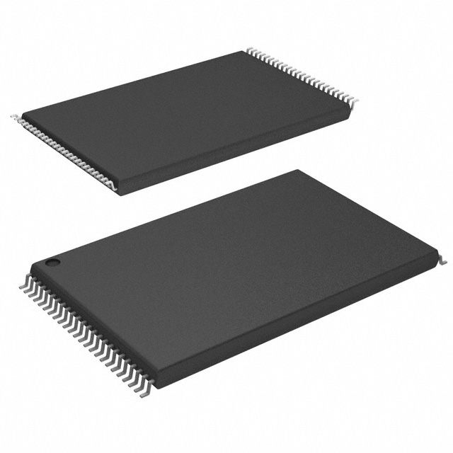
CY62167ELL-45ZXI
ActiveSRAM, ASYNCHRONOUS SRAM, 16 MBIT, 2M X 8BIT / 1M X 16BIT, TSOP-I, 48 PINS, 4.5 V
Deep-Dive with AI
Search across all available documentation for this part.

CY62167ELL-45ZXI
ActiveSRAM, ASYNCHRONOUS SRAM, 16 MBIT, 2M X 8BIT / 1M X 16BIT, TSOP-I, 48 PINS, 4.5 V
Deep-Dive with AI
Technical Specifications
Parameters and characteristics for this part
| Specification | CY62167ELL-45ZXI |
|---|---|
| Access Time | 45 ns |
| Memory Format | SRAM |
| Memory Interface | Parallel |
| Memory Organization | 2M x 8, 1M x 16 |
| Memory Size | 2 MB |
| Memory Type | Volatile |
| Mounting Type | Surface Mount |
| Operating Temperature [Max] | 85 C |
| Operating Temperature [Min] | -40 ¯C |
| Package / Case | 48-TFSOP |
| Package / Case [x] | 0.724 in |
| Package / Case [y] | 18.4 mm |
| Supplier Device Package | 48-TSOP I |
| Technology | SRAM - Asynchronous |
| Voltage - Supply [Max] | 5.5 V |
| Voltage - Supply [Min] | 4.5 V |
| Write Cycle Time - Word, Page [custom] | 45 ns |
| Write Cycle Time - Word, Page [custom] | 45 ns |
Pricing
Prices provided here are for design reference only. For realtime values and availability, please visit the distributors directly
| Distributor | Package | Quantity | $ | |
|---|---|---|---|---|
| Arrow | N/A | 1 | $ 9.49 | |
| Digikey | Bulk | 26 | $ 11.92 | |
| 26 | $ 11.92 | |||
| N/A | 193 | $ 16.15 | ||
| 193 | $ 16.15 | |||
| 227 | $ 13.56 | |||
| 227 | $ 13.56 | |||
| 302 | $ 9.40 | |||
| 302 | $ 9.40 | |||
| Tray | 1 | $ 15.71 | ||
| 1 | $ 15.71 | |||
| 10 | $ 14.54 | |||
| 10 | $ 14.54 | |||
| 25 | $ 14.34 | |||
| 25 | $ 14.34 | |||
| 40 | $ 14.16 | |||
| 40 | $ 14.16 | |||
| 96 | $ 12.41 | |||
| 96 | $ 12.41 | |||
| 288 | $ 11.88 | |||
| 288 | $ 11.88 | |||
| 480 | $ 11.80 | |||
| 480 | $ 11.80 | |||
| Newark | Each | 1 | $ 13.26 | |
| 10 | $ 12.67 | |||
| 25 | $ 12.00 | |||
| 50 | $ 11.49 | |||
| 100 | $ 11.35 | |||
| 250 | $ 11.19 | |||
| 500 | $ 10.36 | |||
Description
General part information
CY62167 Series
CY62167ELL-45ZXI is a high-performance CMOS static RAM organized as 1M words by 16 bits/2M words by 8 bits. This device features an advanced circuit design to provide an ultra-low active current. This is ideal for providing More Battery Life (MoBL®) in portable applications. This device also has an automatic power down feature that reduces power consumption when addresses are not toggling. To write to the device, take chip enables (active-low CE1 LOW and CE2 HIGH) and write enable (active-low WE) input LOW. If byte low enable (active-low BLE) is LOW, then data from I/O pins (I/O0 through I/O7), is written into the location specified on the address pins (A0 through A19). If byte high enable (active-low BHE) is LOW, then data from the I/O pins (I/O8 through I/O15) is written into the location specified on the address pins (A0 through A19).
Documents
Technical documentation and resources


