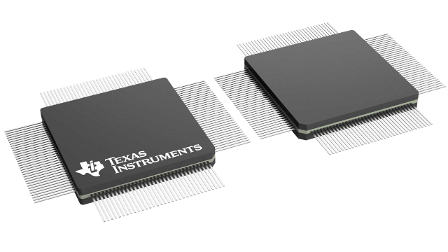
SN54ACT3632HFP
Obsolete512 X 36 X 2 SYNCHRONOUS BIDIRECTIONAL FIFO MEMORY
Deep-Dive with AI
Search across all available documentation for this part.

SN54ACT3632HFP
Obsolete512 X 36 X 2 SYNCHRONOUS BIDIRECTIONAL FIFO MEMORY
Deep-Dive with AI
Technical Specifications
Parameters and characteristics for this part
| Specification | SN54ACT3632HFP |
|---|---|
| Access Time | 15 ns |
| Bus Directional | Bi-Directional |
| Current - Supply (Max) [Max] | 400 µA |
| Data Rate | 50 MHz |
| Function | Synchronous |
| FWFT Support | False |
| Memory Size | 36 K |
| Mounting Type | Surface Mount |
| Operating Temperature [Max] | 125 °C |
| Operating Temperature [Min] | -55 °C |
| Package / Case | 132-CFlatPack |
| Programmable Flags Support | True |
| Retransmit Capability | False |
| Supplier Device Package | 132-CFP (24.13x24.13) |
| Voltage - Supply [Max] | 5.5 V |
| Voltage - Supply [Min] | 4.5 V |
Pricing
Prices provided here are for design reference only. For realtime values and availability, please visit the distributors directly
| Distributor | Package | Quantity | $ | |
|---|---|---|---|---|
| Texas Instruments | TUBE | 1 | $ 471.38 | |
| 10 | $ 432.10 | |||
| 100 | $ 392.82 | |||
Description
General part information
SN54ACT3632 Series
The SN54ACT3632 is a high-speed, low-power CMOS clocked bidirectional FIFO memory. It supports clock frequencies up to 50 MHz and has read access times as fast as 11 ns. Two independent 512 × 36 dual-port SRAM FIFOs on the chip buffer data in opposite directions. Each FIFO has flags to indicate empty and full conditions and two programmable flags (almost full and almost empty) to indicate when a selected number of words is stored in memory. Communication between each port can bypass the FIFOs via two 36-bit mailbox registers. Each mailbox register has a flag to signal when new mail has been stored. Two or more devices can be used in parallel to create wider data paths.
The SN54ACT3632 is a clocked FIFO, which means each port employs a synchronous interface. All data transfers through a port are gated to the low-to-high transition of a port clock by enable signals. The clocks for each port are independent of one another and can be asynchronous or coincident. The enables for each port are arranged to provide a simple bidirectional interface between microprocessors and/or buses with synchronous control.
The input-ready (IRA, IRB) flag and almost-full (AFA\, AFB\) flag of a FIFO are two-stage synchronized to the port clock that writes data to its array. The output-ready (ORA, ORB) flag and almost-empty (AEA\, AEB\) flag of a FIFO are two-stage synchronized to the port clock that reads data from its array. Offset values for the almost-full and almost-empty flags of both FIFOs can be programmed from port A.
Documents
Technical documentation and resources


