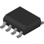
MAX5063AASA+
ActiveDRIVER 2A 2-OUT HIGH SIDE/LOW SIDE HALF BRDG NON-INV 8-PIN SOIC N TUBE
Deep-Dive with AI
Search across all available documentation for this part.

MAX5063AASA+
ActiveDRIVER 2A 2-OUT HIGH SIDE/LOW SIDE HALF BRDG NON-INV 8-PIN SOIC N TUBE
Deep-Dive with AI
Technical Specifications
Parameters and characteristics for this part
| Specification | MAX5063AASA+ |
|---|---|
| Channel Type | Independent |
| Current - Peak Output (Source, Sink) [custom] | 2 A |
| Current - Peak Output (Source, Sink) [custom] | 2 A |
| Driven Configuration | Half-Bridge |
| Gate Type | N-Channel MOSFET, MOSFET (N-Channel) |
| High Side Voltage - Max (Bootstrap) [Max] | 125 V |
| Input Type | Non-Inverting |
| Logic Voltage - VIL, VIH | 0.8 V, 2 V |
| Mounting Type | Surface Mount |
| Number of Drivers | 2 |
| Operating Temperature [Max] | 150 °C |
| Operating Temperature [Min] | -40 °C |
| Package / Case | 0.154 in |
| Package / Case | 8-SOIC |
| Package / Case | 3.9 mm |
| Rise / Fall Time (Typ) | 65 ns |
| Rise / Fall Time (Typ) | 65 ns |
| Supplier Device Package | 8-SOIC |
| Voltage - Supply [Max] | 12.6 V |
| Voltage - Supply [Min] | 8 V |
Pricing
Prices provided here are for design reference only. For realtime values and availability, please visit the distributors directly
Description
General part information
MAX5063 Series
The MAX5062/MAX5063/MAX5064 high-frequency, 125V half-bridge, n-channel MOSFET drivers drive high-and low-side MOSFETs in high-voltage applications. These drivers are independently controlled and their 35ns typical propagation delay, from input to output, are matched to within 3ns (typ). The high-voltage operation with very low and matched propagation delay between drivers, and high source/sink current capabilities in a thermally enhanced package make these devices suitable for the high-power, high-frequency telecom power converters. The 125V maximum input voltage range provides plenty of margin over the 100V input transient requirement of telecom standards. A reliable on-chip bootstrap diode connected between VDDand BST eliminates the need for an external discrete diode.The MAX5062A/C and the MAX5063A/C offer both noninverting drivers (see theSelector Guideof the full data sheet). The MAX5062B/D and the MAX5063B/D offer a noninverting high-side driver and an inverting low-side driver. The MAX5064A/B offer two inputs per driver that can be either inverting or noninverting. The MAX5062A/B/C/D and the MAX5064A feature CMOS (VDD/ 2) logic inputs. The MAX5063A/B/C/D and the MAX5064B feature TTL logic inputs. The MAX5064A/B include a break-before-make adjustment input that sets the dead time between drivers from 16ns to 95ns. The drivers are available in the industry-standard 8-pin SO footprint and pin configuration, and a thermally enhanced 8-pin SO and 12-pin (4mm x 4mm) thin QFN packages. All devices operate over the -40°C to +125°C automotive temperature range.ApplicationsActive-Clamp Forward ConvertersFull-Bridge ConvertersMotor ControlPower-Supply ModulesTelecom Half-Bridge Power SuppliesTwo-Switch Forward Converters
Documents
Technical documentation and resources


