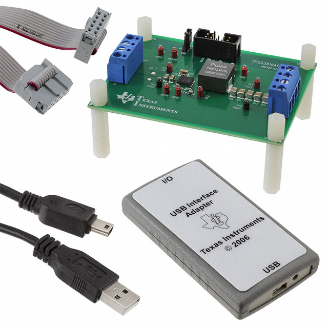
TPS53819AEVM-123
ActiveEVAL BOARD FOR TPS53819A
Deep-Dive with AI
Search across all available documentation for this part.

TPS53819AEVM-123
ActiveEVAL BOARD FOR TPS53819A
Deep-Dive with AI
Technical Specifications
Parameters and characteristics for this part
| Specification | TPS53819AEVM-123 |
|---|---|
| Board Type | Fully Populated |
| Contents | Board(s) |
| Current - Output | 25 A |
| Frequency - Switching | 425 kHz |
| Main Purpose | DC/DC, Step Down |
| Outputs and Type | 1 Non-Isolated Output, Non-Isolated |
| Outputs and Type | 1 |
| Regulator Topology | Buck |
| Supplied Contents | Board(s) |
| Utilized IC / Part | TPS53819A |
| Voltage - Input [Max] | 14 V |
| Voltage - Input [Min] | 8 V |
| Voltage - Output | 1.2 V |
Pricing
Prices provided here are for design reference only. For realtime values and availability, please visit the distributors directly
| Distributor | Package | Quantity | $ | |
|---|---|---|---|---|
| Digikey | Box | 1 | $ 238.80 | |
Description
General part information
TPS53819A Series
The TPS53819A device is a small-sized, single buck controller with adaptive on-time D-CAP2 mode control and PMBus. The device is suitable for low output voltage and high current, system power rail, or similar point-of-load (POL) power supply in digital consumer products. Small package with minimal pin-count saves space on the PCB, while the programmability and fault report via PMBus simplify the power supply design. The skip-mode at light-load condition combined with strong gate drivers and low-side FET on-resistance (RDS(on)) current sensing can support low-loss and high efficiency operation, over a broad load range. The conversion input voltage, which is the high-side FET drain voltage, ranges from 3 V to 28 V. The supply voltage (VDD) is from 4.5 V to 28 V. The output voltage ranges from 0.6 V to 5.5 V. The device is available in a 16-pin, QFN package and is specified from –40°C to +85°C.
The TPS53819A device is a small-sized, single buck controller with adaptive on-time D-CAP2 mode control and PMBus. The device is suitable for low output voltage and high current, system power rail, or similar point-of-load (POL) power supply in digital consumer products. Small package with minimal pin-count saves space on the PCB, while the programmability and fault report via PMBus simplify the power supply design. The skip-mode at light-load condition combined with strong gate drivers and low-side FET on-resistance (RDS(on)) current sensing can support low-loss and high efficiency operation, over a broad load range. The conversion input voltage, which is the high-side FET drain voltage, ranges from 3 V to 28 V. The supply voltage (VDD) is from 4.5 V to 28 V. The output voltage ranges from 0.6 V to 5.5 V. The device is available in a 16-pin, QFN package and is specified from –40°C to +85°C.
Documents
Technical documentation and resources


