Deep-Dive with AI
Search across all available documentation for this part.

Deep-Dive with AI
Technical Specifications
Parameters and characteristics for this part
| Specification | SN74AVC16646DGG |
|---|---|
| Current - Output High, Low [custom] | 12 mA |
| Current - Output High, Low [custom] | 12 mA |
| Mounting Type | Surface Mount |
| Number of Bits per Element [custom] | 8 |
| Number of Elements | 2 |
| Operating Temperature [Max] | 85 C |
| Operating Temperature [Min] | -40 ¯C |
| Output Type | 3-State |
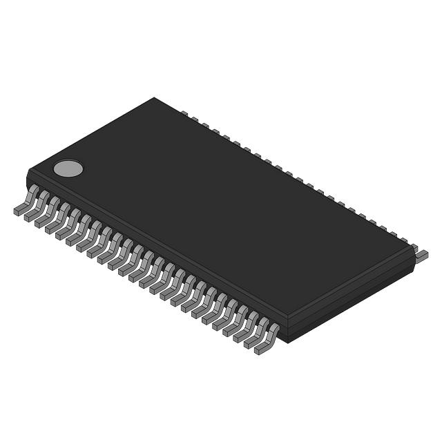
| Package / Case | 56-TFSOP |
| Package / Case [x] | 0.24 in |
| Package / Case [y] | 6.1 mm |
| Supplier Device Package | 56-TSSOP |
| Voltage - Supply [Max] | 3.6 V |
| Voltage - Supply [Min] | 1.2 V |
Pricing
Prices provided here are for design reference only. For realtime values and availability, please visit the distributors directly
| Distributor | Package | Quantity | $ | |
|---|---|---|---|---|
| Digikey | Bulk | 210 | $ 1.44 | |
| N/A | 1121 | $ 1.73 | ||
Description
General part information
74AVC16646 Series
A Dynamic Output Control (DOC) circuit is implemented, which, during the transition, initially lowers the output impedance to effectively drive the load and, subsequently, raises the impedance to reduce noise. Figure 1 shows typical VOLvs IOLand VOHvs IOHcurves to illustrate the output impedance and drive capability of the circuit. At the beginning of the signal transition, the DOC circuit provides a maximum dynamic drive that is equivalent to a high-drive standard-output device. For more information, refer to the TI application reports,AVC Logic Family Technology and Applications, literature number SCEA006, andDynamic Output Control (DOCTM) Circuitry Technology and Applications, literature number SCEA009.
This 16-bit bus transceiver and register is operational at 1.2-V to 3.6-V VCC, but is designed specifically for 1.65-V to 3.6-V VCCoperation.
The SN74AVC16646 can be used as two 8-bit transceivers or one 16-bit transceiver. Data on the A or B bus is clocked into the registers on the low-to-high transition of the appropriate clock (CLKAB or CLKBA) input. Figure 2 illustrates the four fundamental bus-management functions that can be performed with the SN74AVC16646.
Documents
Technical documentation and resources
No documents available


