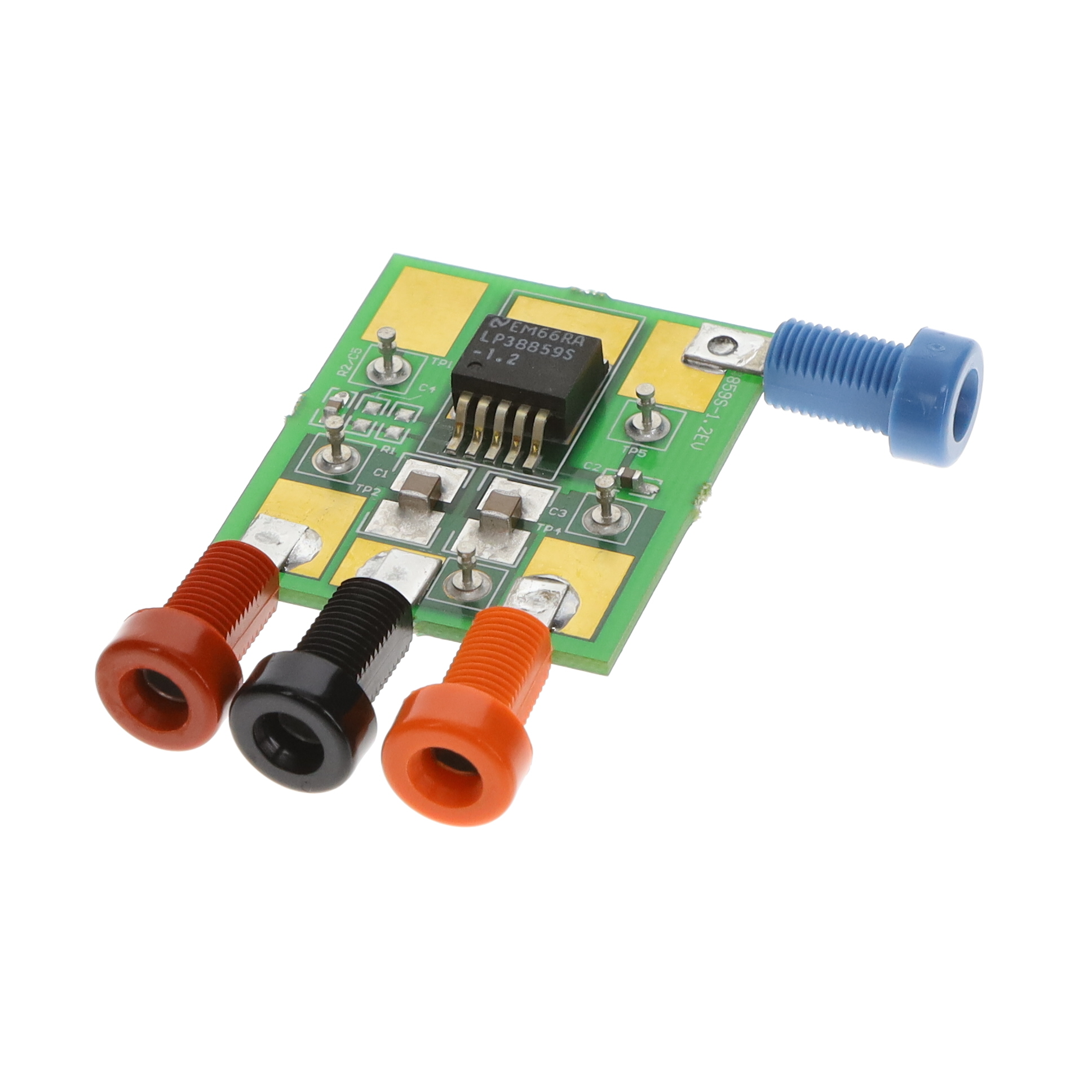
LP38859-1.2EVAL
ObsoleteBOARD EVALUATION LP38859-1.2
Deep-Dive with AI
Search across all available documentation for this part.

LP38859-1.2EVAL
ObsoleteBOARD EVALUATION LP38859-1.2
Deep-Dive with AI
Technical Specifications
Parameters and characteristics for this part
| Specification | LP38859-1.2EVAL |
|---|---|
| Board Type | Fully Populated |
| Channels per IC | 1 - Single |
| Current - Output | 3 A |
| Regulator Type | Positive Fixed |
| Supplied Contents | Board(s) |
| Utilized IC / Part | LP38859 |
| Voltage - Input [Max] | 5.5 V |
| Voltage - Input [Min] | 3 V |
| Voltage - Output | 1.2 V |
Pricing
Prices provided here are for design reference only. For realtime values and availability, please visit the distributors directly
| Distributor | Package | Quantity | $ | |
|---|---|---|---|---|
| Digikey | Box | 1 | $ 26.40 | |
Description
General part information
LP38859 Series
The LP38859 is a high-current, fast-response regulator which can maintain output voltage regulation with extremely low input to output voltage drop. Fabricated on a CMOS process, the device operates from two input voltages: VBIASprovides voltage to drive the gate of the N-MOS power transistor, while VINis the input voltage which supplies power to the load. The use of an external bias rail allows the part to operate from ultra-low VINvoltages. Unlike bipolar regulators, the CMOS architecture consumes extremely low quiescent current at any output load current. The use of an N-MOS power transistor results in wide bandwidth, yet minimum external capacitance is required to maintain loop stability.
The fast transient response of this device makes it suitable for use in powering DSP microcontroller core voltages and switch-mode power-supply post-regulators. The LP38859 is available in 5-pin TO-220 and DDPAK/TO-263 packages.
The LP38859 is a high-current, fast-response regulator which can maintain output voltage regulation with extremely low input to output voltage drop. Fabricated on a CMOS process, the device operates from two input voltages: VBIASprovides voltage to drive the gate of the N-MOS power transistor, while VINis the input voltage which supplies power to the load. The use of an external bias rail allows the part to operate from ultra-low VINvoltages. Unlike bipolar regulators, the CMOS architecture consumes extremely low quiescent current at any output load current. The use of an N-MOS power transistor results in wide bandwidth, yet minimum external capacitance is required to maintain loop stability.
Documents
Technical documentation and resources
No documents available


