Deep-Dive with AI
Search across all available documentation for this part.

Deep-Dive with AI
Technical Specifications
Parameters and characteristics for this part
| Specification | SN65LVDT122PWRG4 |
|---|---|
| Circuit | 1 x 2:2 |
| Independent Circuits | 1 |
| Mounting Type | Surface Mount |
| Operating Temperature [Max] | 85 °C |
| Operating Temperature [Min] | -40 °C |
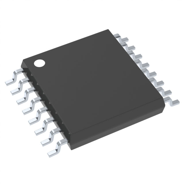
| Package / Case | 16-TSSOP |
| Package / Case [x] | 0.173 in |
| Package / Case [y] | 4.4 mm |
| Supplier Device Package | 16-TSSOP |
| Type | Crosspoint Switch |
| Voltage - Supply [Max] | 3.6 V |
| Voltage - Supply [Min] | 3 V |
| Voltage Supply Source | Single Supply |
Pricing
Prices provided here are for design reference only. For realtime values and availability, please visit the distributors directly
| Distributor | Package | Quantity | $ | |
|---|---|---|---|---|
Description
General part information
SN65LVDT122 Series
The SN65LVDS122 and SN65LVDT122 are crosspoint switches that use low voltage differential signaling (LVDS) to achieve signaling rates as high as 1.5 Gbps. They are pin-compatible speed upgrades to the SN65LVDS22 and SN65LVDM22. The internal signal paths maintain differential signaling for high speeds and low signal skews. These devices have a 0 V to 4 V common-mode input range that accepts LVDS, LVPECL, CML inputs. Two logic pins (S0 and S1) set the internal configuration between the differential inputs and outputs. This allows the flexibility to perform the following configurations: 2 x 2 crosspoint switch, 2:1 mux, 1:2 splitter or dual repeater/translator within a single device. Additionally, SN65LVDT122 incorporates a 110-termination resistor for those applications where board space is a premium. Although these devices are designed for 1.5 Gbps, some applications at a 2-Gbps data rate can be supported depending on loading and signal quality.
The intended application of this device is ideal for loopback switching for diagnostic routines, fanout buffering of clock/data distribution provide protection in fault-tolerant systems, clock muxing in optical modules, and for overall signal boosting over extended distances.
The SN65LVDS122 and SN65LVDT122 are characterized for operation from –40°C to 85°C.
Documents
Technical documentation and resources
No documents available


