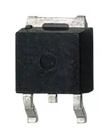
IPD19DP10NMATMA1
ActiveIPD19DP10NM P-CHANNEL MOSFETS IN NORMAL LEVEL IN DPAK
Deep-Dive with AI
Search across all available documentation for this part.

IPD19DP10NMATMA1
ActiveIPD19DP10NM P-CHANNEL MOSFETS IN NORMAL LEVEL IN DPAK
Deep-Dive with AI
Technical Specifications
Parameters and characteristics for this part
| Specification | IPD19DP10NMATMA1 |
|---|---|
| Current - Continuous Drain (Id) @ 25°C | 2.6 A, 13.7 A |
| Drain to Source Voltage (Vdss) | 100 V |
| Drive Voltage (Max Rds On, Min Rds On) | 10 V |
| FET Type | P-Channel |
| Gate Charge (Qg) (Max) @ Vgs | 45 nC |
| Input Capacitance (Ciss) (Max) @ Vds | 2000 pF |
| Mounting Type | Surface Mount |
| Operating Temperature [Max] | 175 °C |
| Operating Temperature [Min] | -55 °C |
| Package / Case | TO-252-3, SC-63, DPAK (2 Leads + Tab) |
| Power Dissipation (Max) | 3 W, 83 W |
| Rds On (Max) @ Id, Vgs | 186 mOhm |
| Supplier Device Package | PG-TO252-3 |
| Technology | MOSFET (Metal Oxide) |
| Vgs (Max) | 20 V |
| Vgs(th) (Max) @ Id | 4 V |
Pricing
Prices provided here are for design reference only. For realtime values and availability, please visit the distributors directly
Description
General part information
IPD19DP10 Series
OptiMOS™ P-channel MOSFETs 100V in DPAKpackage represents the new technology targeted for battery management, load switch and reverse polarity protection applications. The main advantage of a P-channel device is the reduction of design complexity in medium and low power applications. Its easy interface to MCU, fast switching as well as avalanche ruggedness makes it suitable for high quality demanding applications. It is available in logic level featuring a wide RDS(on)range and improves efficiency at low loads due to low Qg.
Documents
Technical documentation and resources


