Deep-Dive with AI
Search across all available documentation for this part.

Deep-Dive with AI
Technical Specifications
Parameters and characteristics for this part
| Specification | SN74LS145DG4 |
|---|---|
| Circuit [custom] | 1 |
| Circuit [custom] | 4:10 |
| Current - Output High, Low | - |
| Current - Output High, Low | 80 mA |
| Independent Circuits | 1 |
| Mounting Type | Surface Mount |
| Operating Temperature [Max] | 70 °C |
| Operating Temperature [Min] | 0 °C |
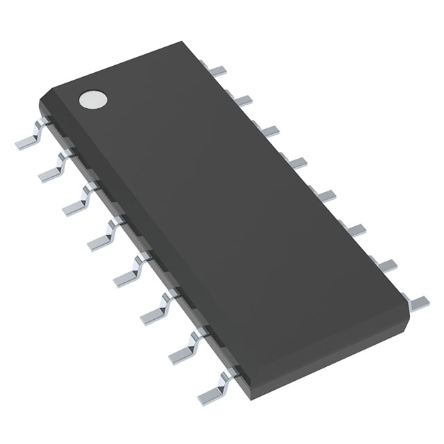
| Package / Case | 16-SOIC |
| Package / Case [x] | 0.154 in |
| Package / Case [y] | 3.9 mm |
| Supplier Device Package | 16-SOIC |
| Type | Decoder |
| Voltage - Supply [Max] | 5.25 V |
| Voltage - Supply [Min] | 4.75 V |
| Voltage Supply Source | Single Supply |
Pricing
Prices provided here are for design reference only. For realtime values and availability, please visit the distributors directly
| Distributor | Package | Quantity | $ | |
|---|---|---|---|---|
Description
General part information
SN74LS145 Series
These monolithic BCD-to-decimal decoder/drivers consist of eight inverters and ten four-input NAND gates. The inverters are connected in pairs to make BCD input date available for decoding by the NAND gates. Full decoding of valid BCD input logic ensures that all outputs remain off for all invalid binary input conditions. These decoders feature high-performance,n-p-n output transistors designed for use as indicator/relay drivers or as open-collector logic-circuit drivers. Each of the high-breakdown output transistors (15 volts) of the SN54145, SN74145, or SN74LS145 will sink up to 80 milliamperes of current. Each input is one Series 54/74 or Series 54LS/74LS standard load, respectively. Inputs and outputs are entirely compatible for use with TTL or DTL logic curciuts, and the outputs are compatible for interfacing with most MOS integrated circuits. Power dissipation is typically 215 milliwatts for the '145 and 35 milliwatts for the 'LS145.
These monolithic BCD-to-decimal decoder/drivers consist of eight inverters and ten four-input NAND gates. The inverters are connected in pairs to make BCD input date available for decoding by the NAND gates. Full decoding of valid BCD input logic ensures that all outputs remain off for all invalid binary input conditions. These decoders feature high-performance,n-p-n output transistors designed for use as indicator/relay drivers or as open-collector logic-circuit drivers. Each of the high-breakdown output transistors (15 volts) of the SN54145, SN74145, or SN74LS145 will sink up to 80 milliamperes of current. Each input is one Series 54/74 or Series 54LS/74LS standard load, respectively. Inputs and outputs are entirely compatible for use with TTL or DTL logic curciuts, and the outputs are compatible for interfacing with most MOS integrated circuits. Power dissipation is typically 215 milliwatts for the '145 and 35 milliwatts for the 'LS145.
Documents
Technical documentation and resources
No documents available


