Deep-Dive with AI
Search across all available documentation for this part.

Deep-Dive with AI
Technical Specifications
Parameters and characteristics for this part
| Specification | DS90C365AMT |
|---|---|
| Data Rate | 1.785 Gbps |
| Mounting Type | Surface Mount |
| Number of Drivers/Receivers [custom] | 4 |
| Number of Drivers/Receivers [custom] | 0 |
| Operating Temperature [Max] [custom] | 158 °F |
| Operating Temperature [Min] [custom] | -10 °C |
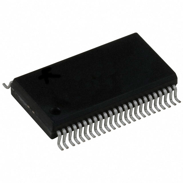
| Package / Case | 48-TFSOP |
| Package / Case | 0.24 in |
| Package / Case [custom] | 6.1 mm |
| Protocol | LVDS, FPD-Link |
| Supplier Device Package | 48-TSSOP |
| Type | Driver |
| Voltage - Supply [Max] | 3.6 V |
| Voltage - Supply [Min] | 3 V |
Pricing
Prices provided here are for design reference only. For realtime values and availability, please visit the distributors directly
| Distributor | Package | Quantity | $ | |
|---|---|---|---|---|
Description
General part information
DS90C365A Series
The DS90C365A is a pin to pin compatible replacement for DS90C363, DS90C363A and DS90C365. The DS90C365A has additional features and improvements making it an ideal replacement for DS90C363, DS90C363A and DS90C365. family of LVDS Transmitters.
The DS90C365A transmitter converts 21 bits of LVCMOS/LVTTL data into four LVDS (Low Voltage Differential Signaling) data streams. A phase-locked transmit clock is transmitted in parallel with the data streams over the fourth LVDS link. Every cycle of the transmit clock 21 bits RGB of input data are sampled and transmitted. At a transmit clock frequency of 87.5 MHz, 21 bits of RGB data and 3 bits of LCD timing and control data (FPLINE, FPFRAME, DRDY) are transmitted at a rate of 612.5 Mbps per LVDS data channel. Using a 87.5 MHz clock, the data throughput is 229.687 Mbytes/sec. This transmitter can be programmed for Rising edge strobe or Falling edge strobe through a dedicated pin. A Rising edge or Falling edge strobe transmitter will interoperate with a Falling edge strobe FPDLink Receiver without any translation logic.
This chipset is an ideal means to solve EMI and cable size problems associated with wide, high-speed TTL interfaces with added Spead Spectrum Clocking support..
Documents
Technical documentation and resources
No documents available


