Deep-Dive with AI
Search across all available documentation for this part.

Deep-Dive with AI
Technical Specifications
Parameters and characteristics for this part
| Specification | 74VHC112SJX |
|---|---|
| Clock Frequency | 185 MHz |
| Current - Output High, Low [custom] | 8 mA |
| Current - Output High, Low [custom] | 8 mA |
| Current - Quiescent (Iq) | 2 µA |
| Function | Reset, Set(Preset) |
| Input Capacitance | 4 pF |
| Max Propagation Delay @ V, Max CL | 10.5 ns |
| Mounting Type | Surface Mount |
| Number of Bits per Element | 1 |
| Number of Elements | 2 |
| Operating Temperature [Max] | 85 °C |
| Operating Temperature [Min] | -40 °C |
| Output Type | Complementary |
| Package / Case | 0.209 " |
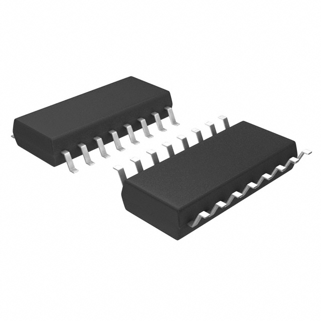
| Package / Case | 16-SOIC |
| Package / Case | 5.3 mm |
| Supplier Device Package | 16-SOP |
| Trigger Type | Negative Edge |
| Type | JK Type |
| Voltage - Supply [Max] | 5.5 V |
| Voltage - Supply [Min] | 2 V |
Pricing
Prices provided here are for design reference only. For realtime values and availability, please visit the distributors directly
| Distributor | Package | Quantity | $ | |
|---|---|---|---|---|
Description
General part information
74VHC112 Series
The VHC112 is an advanced high speed CMOS device fabricated with silicon gate CMOS technology. It achieves the high-speed operation similar to equivalent Bipolar Schottky TTL while maintaining the CMOS low power dissipation. The VHC112 contains two independent, high-speed JK flip-flops with Direct Set and Clear inputs. Synchronous state changes are initiated by the falling edge of the clock. Triggering occurs at a voltage level of the clock and is not directly related to transition time. The J and K inputs can change when the clock is in either state without affecting the flip-flop, provided that they are in the desired state during the recommended setup and hold times relative to the falling edge of the clock. The LOW signal on PR or CLR prevents clocking and forces Q and Q# HIGH, respectively. Simultaneous LOW signals on PR and CLR force both Q and Q# HIGH. An input protection circuit ensures that 0V to 7V can be applied to the input pins without regard to the supply voltage. This device can be used to interface 5V to 3V systems and two supply systems such as battery backup. This circuit prevents device destruction due to mismatched supply and input voltages.
Documents
Technical documentation and resources
No documents available


