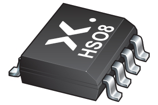
NGD4300DD-Q100J
Active4 A PEAK HIGH-PERFORMANCE DUAL MOSFET GATE DRIVER
Deep-Dive with AI
Search across all available documentation for this part.

NGD4300DD-Q100J
Active4 A PEAK HIGH-PERFORMANCE DUAL MOSFET GATE DRIVER
Technical Specifications
Parameters and characteristics for this part
| Specification | NGD4300DD-Q100J |
|---|---|
| Channel Type | Independent |
| Current - Peak Output (Source, Sink) | 5 A, 4 A |
| Driven Configuration | Half-Bridge |
| Gate Type | MOSFET (N-Channel) |
| Grade | Automotive |
| High Side Voltage - Max (Bootstrap) [Max] | 120 V |
| Input Type | Non-Inverting |
| Mounting Type | Surface Mount |
| Number of Drivers | 2 |
| Operating Temperature [Max] | 125 °C |
| Operating Temperature [Min] | -40 °C |
| Package / Case | Exposed Pad, 8-SOIC |
| Package / Case [x] | 0.154 in |
| Package / Case [y] | 3.9 mm |
| Qualification | AEC-Q100 |
| Rise / Fall Time (Typ) [custom] | 3.5 ns |
| Rise / Fall Time (Typ) [custom] | 4 ns |
| Supplier Device Package | 8-HSO |
| Voltage - Supply [Max] | 17 V |
| Voltage - Supply [Min] | 8 V |
Pricing
Prices provided here are for design reference only. For realtime values and availability, please visit the distributors directly
| Distributor | Package | Quantity | $ | |
|---|---|---|---|---|
| Digikey | N/A | 2638 | $ 1.78 | |
Description
General part information
NGD4300DD-Q100 Series
The NGD4300-Q100 is a high-performance gate driver designed to drive both high-side and low-side N-channel MOSFETs in a synchronous buck or a half-bridge configuration. The floating high-side driver can work with rail voltages up to 120 V and uses a bootstrap supply with an integrated diode. Both low-side and high-side output drivers have an independent undervoltage lockout (UVLO) circuit which disables the output driver when the driver supply is below its threshold level. The NGD4300-Q100 accepts input control signals complying with both TTL and CMOS signaling as low as 2.5 V (±10%). The low voltage, provided by an internal voltage regulator, is used to supply circuitry in signal paths controlling the low-side and high-side power switches. This enables a low-power operation and a better controlled driver performance irrespective of the IC supply voltage.
Documents
Technical documentation and resources


