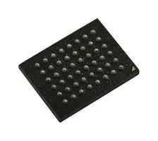
S29JL032J70BHI310
LTBFLASH MEMORY, PARALLEL NOR, 32 MBIT, 2M X 16BIT / 4M X 8BIT, PARALLEL, FBGA, 48 PINS
Deep-Dive with AI
Search across all available documentation for this part.

S29JL032J70BHI310
LTBFLASH MEMORY, PARALLEL NOR, 32 MBIT, 2M X 16BIT / 4M X 8BIT, PARALLEL, FBGA, 48 PINS
Deep-Dive with AI
Technical Specifications
Parameters and characteristics for this part
| Specification | S29JL032J70BHI310 |
|---|---|
| Access Time | 70 ns |
| Memory Format | FLASH |
| Memory Interface | Parallel |
| Memory Organization | 2M x 16, 4M x 8 |
| Memory Size | 4 MB |
| Memory Type | Non-Volatile |
| Mounting Type | Surface Mount |
| Operating Temperature [Max] | 85 C |
| Operating Temperature [Min] | -40 ¯C |
| Package / Case | 48-VFBGA |
| Supplier Device Package | 48-FBGA |
| Supplier Device Package [x] | 8.15 |
| Supplier Device Package [y] | 6.15 |
| Technology | FLASH - NOR |
| Voltage - Supply [Max] | 3.6 V |
| Voltage - Supply [Min] | 2.7 V |
| Write Cycle Time - Word, Page | 70 ns |
Pricing
Prices provided here are for design reference only. For realtime values and availability, please visit the distributors directly
Description
General part information
S29JL032J Series
S29JL032J70BHI310 is a S29JL032J 32Mb (4M × 8Bit/2M × 16Bit), 3V, simultaneous read/write flash memory. Word mode data appears on DQ15–DQ0; byte mode data appears on DQ7–DQ0. The device is designed to be programmed in-system with the standard 3.0 volt VCC supply, and can also be programmed in standard EPROM programmers. Standard control pins—chip enable (CE#), write enable (WE#), and output enable (OE#)—control normal read and write operations, and avoid bus contention issues. The device requires only a single 3.0 volt power supply for both read and write functions. Internally generated and regulated voltages are provided for the program and erase operations.
Documents
Technical documentation and resources


