D
Diodes Inc
| Series | Category | # Parts | Status | Description |
|---|---|---|---|---|
| Part | Spec A | Spec B | Spec C | Spec D | Description |
|---|---|---|---|---|---|
| Series | Category | # Parts | Status | Description |
|---|---|---|---|---|
| Part | Spec A | Spec B | Spec C | Spec D | Description |
|---|---|---|---|---|---|
| Part | Category | Description |
|---|---|---|
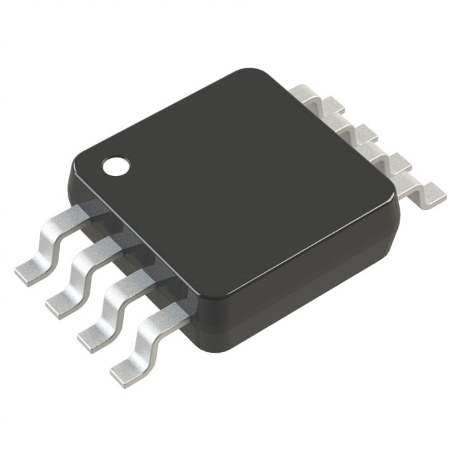 Diodes Inc ZXSC100X8TAObsolete | Integrated Circuits (ICs) | SWITCHING CONTROLLER, VOLTAGE-MODE, 200KHZ SWITCHING FREQ-MAX, PDSO8, MSOP-8 |
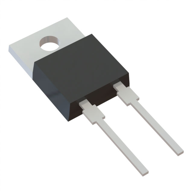 Diodes Inc MBR1045Obsolete | Discrete Semiconductor Products | DIODE SCHOTTKY 45V 10A TO220AC |
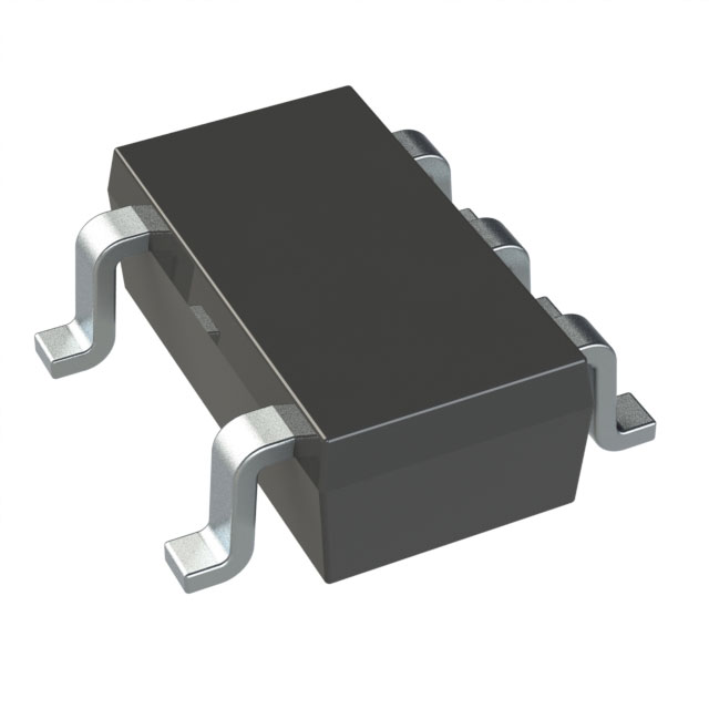
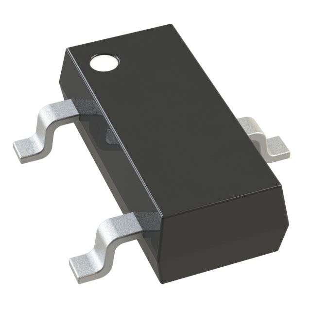 Diodes Inc | Discrete Semiconductor Products | TRANS GP BJT NPN 45V 0.1A 3-PIN SOT-23 T/R |
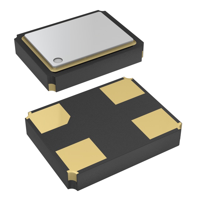 Diodes Inc | Crystals Oscillators Resonators | CRYSTAL 25MHZ FUND 60OHM 4-PIN MINI-CSMD |
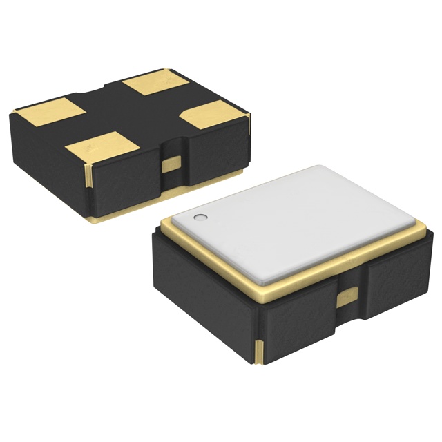 Diodes Inc | Crystals Oscillators Resonators | XTAL OSC XO 133.0000MHZ CMOS SMD |
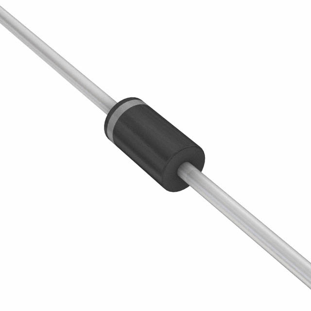 Diodes Inc | Discrete Semiconductor Products | DIODE GEN PURP 100V 1A DO41 |
Diodes Inc MBRF20150CTLObsolete | Discrete Semiconductor Products | DIODE SCHOTTKY ITO220AB |
 Diodes Inc | Integrated Circuits (ICs) | NRND = NOT RECOMMENDED FOR NEW DESIGN |
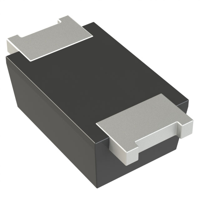 Diodes Inc | Discrete Semiconductor Products | 1.1V@2A 240NS INDEPENDENT TYPE 1A 1KV SOD-123F FAST RECOVERY / HIGH EFFICIENCY DIODES ROHS |
 Diodes Inc | Integrated Circuits (ICs) | ANALOGUE SW, SPDT, -40 TO 125DEG C ROHS COMPLIANT: YES |
| Series | Category | # Parts | Status | Description |
|---|---|---|---|---|
74LVC1G11Single 3 Input AND Gate | Gates and Inverters | 3 | Active | TN1.pdf |
74LVC1G125QSingle Buffer, 3-State, OE LOW | Logic | 2 | Active | The 74LVC1G125Q an automotive-compliant single, non-inverting buffer/bus driver with a 3-state output. The output enters a high-impedance state when a HIGH level is applied to the output enable (OE) pin. The device is designed for operation with a power supply range of 1.65V to 5.5V. The inputs are tolerant to 5.5V, allowing this device to be used in a mixed-voltage environment. The device is fully specified for partial power-down applications using IOFF. The IOFF circuitry disables the output preventing damaging current backflow when the device is powered down. |
74LVC1G126Single Buffer, 3-State, OE HIGH | Integrated Circuits (ICs) | 2 | Active | The 74LVC1G126 is a single non-inverting buffer/bus driver with a 3-state output. The output enters a high impedance state when a LOW-level is applied to the output enable (OE) pin. The device is designed for operation with a power supply range of 1.65V to 5.5V. The inputs are tolerant to 5.5V allowing this device to be used in a mixed voltage environment. The device is fully specified for partial power down applications using IOFF. The IOFFcircuitry disables the output preventing damaging current backflow when the device is powered down. |
74LVC1G14QSchmitt Trigger Inverter | Integrated Circuits (ICs) | 4 | Active | The 74LVC1G14Q is an automotive-compliant, single 1-input Schmitt trigger inverter with a standard push-pull output. The device is designed for operation with a power supply range of 1.65V to 5.5V. The inputs are tolerant to 5.5V allowing this device to be used in a mixed-voltage environment. The device is fully specified for partial power down applications using IOFF. The IOFF circuitry disables the output preventing damaging current backflow when the device is powered down. |
74LVC1G17QSchmitt Trigger Single Buffer | Buffers, Drivers, Receivers, Transceivers | 5 | Active | The 74LVC1G17 is a single 1-input Schmitt-trigger buffer with a standard push-pull output. The device is designed for operation with a power supply range of 1.65V to 5.5V. The inputs are tolerant to 5.5V allowing this device to be used in a mixed voltage environment. The device is fully specified for partial power down applications using IOFF. The IOFF circuitry disables the output preventing damaging current backflow when the device is powered down. The gate performs the positive Boolean function: Y = A |
74LVC1G32Single 2 Input OR Gate | Logic | 2 | Active | The 74LVC1G32 is a single 2-input positive OR gate with a standard totem pole output. The device is designed for operation with a power supply range of 1.65V to 5.5V. The inputs are tolerant to 5.5V allowing this device to be used in a mixed voltage environment. The device is fully specified for partial power down applications using IOFF. The IOFFcircuitry disables the output preventing damaging current backflow when the device is powered down. |
74LVC1G34QSingle Buffer | Logic | 6 | Active | The 74LVC1G34Q is an automotive-compliant, single buffer gate with a standard push-pull output. The device is designed for operation with a power supply range of 1.65V to 5.5V. The inputs are tolerant to 5.5V allowing this device to be used in a mixed voltage environment. The device is fully specified for partial power down applications using IOFF. The IOFF circuitry disables the output preventing damaging current backflow when the device is powered down. |
74LVC1G57Multi-Functional Gate, Configurable, 3 Input | Gates and Inverters - Multi-Function, Configurable | 1 | Active | TN1.pdf |
74LVC1G86QSingle 2 Inut XOR Gate | Integrated Circuits (ICs) | 9 | Active | The 74LVC1G86 is a single 2-input EXCLUSIVE OR gate with a standard totem pole output. The device is designed for operation with a power supply range of 1.65V to 5.5V. The inputs are tolerant to 5.5V allowing this device to be used in a mixed voltage environment. The device is fully specified for partial power down applications using IOFF. The IOFFcircuitry disables the output preventing damaging current backflow when the device is powered down. The gate performs the positive Boolean function: Y = A ⊕B or Y = AB + AB |
74LVC1G97Multi-Functional Gate, Configurable, 3 Input | Integrated Circuits (ICs) | 2 | Active | The 74LVC1G97 is a single three-input positive configurable multiple-function gate with a standard push-pull output. The output state is determined by eight patterns of three-bit input. The user can choose the logic functions MUX, AND, OR, NAND, NOR, inverter or noninverting buffer. All inputs can be connected to ground or VCCas required. The device is designed for operation with a power supply range of 1.65V to 5.5V. The inputs are tolerant to 5.5V allowing this device to be used in a mixed voltage environment. The device is fully specified for partial power-down applications using IOFF. The IOFF circuitry disables the output to prevent damaging current backflow when the device is powered down. The user is reminded that the device can simulate several types of logic gates but may respond differently due to the Schmitt action at the inputs. |


