DS90C124-Q1 Series
5-MHz to 35-MHz DC-balanced 24-bit automotive FPD-Link II deserializer
Manufacturer: Texas Instruments
Catalog
5-MHz to 35-MHz DC-balanced 24-bit automotive FPD-Link II deserializer
Key Features
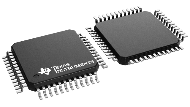
• 5-MHz to 35-MHz Clock Embedded and DC-Balancing 24:1 and 1:24 Data TransmissionsUser Defined Pre-Emphasis Driving Ability Through External Resistor on LVDS Outputs and Capable to Drive Up to 10-Meter Shielded Twisted-Pair CableUser-Selectable Clock Edge for Parallel Data on Both Transmitter and ReceiverInternal DC Balancing Encode and Decode (Supports AC-Coupling Interface With No External Coding Required)Individual Power-Down Controls for Both Transmitter and ReceiverEmbedded Clock CDR (Clock and Data Recovery) on Receiver and No External Source of Reference Clock RequiredAll Codes RDL (Random Data Lock) to Support Live-Pluggable ApplicationsLOCK Output Flag to Ensure Data Integrity at Receiver SideBalanced TSETUPand THOLDBetween RCLK and RDATA on Receiver SidePTO (Progressive Turnon) LVCMOS Outputs to Reduce EMI and Minimize SSO EffectsAll LVCMOS Inputs and Control Pins Have Internal PulldownOn-Chip Filters for PLLs on Transmitter and ReceiverTemperature Range: –40°C to 105°CGreater Than 8-kV HBM ESD TolerantMeets AEC-Q100 CompliancePower Supply Range: 3.3 V ± 10%48-Pin TQFP Package5-MHz to 35-MHz Clock Embedded and DC-Balancing 24:1 and 1:24 Data TransmissionsUser Defined Pre-Emphasis Driving Ability Through External Resistor on LVDS Outputs and Capable to Drive Up to 10-Meter Shielded Twisted-Pair CableUser-Selectable Clock Edge for Parallel Data on Both Transmitter and ReceiverInternal DC Balancing Encode and Decode (Supports AC-Coupling Interface With No External Coding Required)Individual Power-Down Controls for Both Transmitter and ReceiverEmbedded Clock CDR (Clock and Data Recovery) on Receiver and No External Source of Reference Clock RequiredAll Codes RDL (Random Data Lock) to Support Live-Pluggable ApplicationsLOCK Output Flag to Ensure Data Integrity at Receiver SideBalanced TSETUPand THOLDBetween RCLK and RDATA on Receiver SidePTO (Progressive Turnon) LVCMOS Outputs to Reduce EMI and Minimize SSO EffectsAll LVCMOS Inputs and Control Pins Have Internal PulldownOn-Chip Filters for PLLs on Transmitter and ReceiverTemperature Range: –40°C to 105°CGreater Than 8-kV HBM ESD TolerantMeets AEC-Q100 CompliancePower Supply Range: 3.3 V ± 10%48-Pin TQFP Package
Description
AI
The DS90C241 and DS90C124 chipset translates a 24-bit parallel bus into a fully transparent data and control LVDS serial stream with embedded clock information. This single serial stream simplifies transferring a 24-bit bus over PCB traces or over cable by eliminating the skew problems between parallel data and clock paths. It saves system cost by narrowing data paths, which in turn reduces PCB layers, cable width, and connector size and pins.
The DS90C241 and DS90C124 incorporate LVDS signaling on the high-speed I/O. LVDS provides a low-power and low-noise environment for reliably transferring data over a serial transmission path. By optimizing the serializer output edge rate for the operating frequency range, EMI is further reduced.
In addition, the device features pre-emphasis to boost signals over longer distances using lossy cables. Internal DC balanced encoding and decoding supports AC-coupled interconnects.


