ADC3421 Series
Quad-channel 12-bit 25-MSPS analog-to-digital converter (ADC)
Manufacturer: Texas Instruments
Catalog
Quad-channel 12-bit 25-MSPS analog-to-digital converter (ADC)
Key Features
• Quad Channel12-Bit ResolutionSingle Supply: 1.8 VSerial LVDS InterfaceFlexible Input Clock Buffer with Divide-by-1, -2, -4SNR = 70.2 dBFS, SFDR = 87 dBc atfIN= 70 MHzUltra-Low Power Consumption:98 mW/Ch at 125 MSPSChannel Isolation: 105 dBInternal Dither and ChopperSupport for Multi-Chip SynchronizationPin-to-Pin Compatible with 14-Bit VersionPackage: VQFN-56 (8 mm × 8 mm)Quad Channel12-Bit ResolutionSingle Supply: 1.8 VSerial LVDS InterfaceFlexible Input Clock Buffer with Divide-by-1, -2, -4SNR = 70.2 dBFS, SFDR = 87 dBc atfIN= 70 MHzUltra-Low Power Consumption:98 mW/Ch at 125 MSPSChannel Isolation: 105 dBInternal Dither and ChopperSupport for Multi-Chip SynchronizationPin-to-Pin Compatible with 14-Bit VersionPackage: VQFN-56 (8 mm × 8 mm)
Description
AI
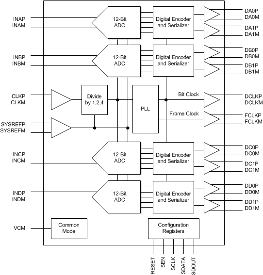
The ADC342x are a high-linearity, ultra-low power, quad-channel, 12-bit, 25-MSPS to 125-MSPS, analog-to-digital converter (ADC) family. The devices are designed specifically to support demanding, high input frequency signals with large dynamic range requirements. An input clock divider allows more flexibility for system clock architecture design and the SYSREF input enables complete system synchronization. The ADC342x family supports serial low-voltage differential signaling (LVDS) in order to reduce the number of interface lines, thus allowing for high system integration density. The serial LVDS interface is two-wire, where each ADC data are serialized and output over two LVDS pairs. An internal phase-locked loop (PLL) multiplies the incoming ADC sampling clock to derive the bit clock that is used to serialize the 12-bit output data from each channel. In addition to the serial data streams, the frame and bit clocks are also transmitted as LVDS outputs.
The ADC342x are a high-linearity, ultra-low power, quad-channel, 12-bit, 25-MSPS to 125-MSPS, analog-to-digital converter (ADC) family. The devices are designed specifically to support demanding, high input frequency signals with large dynamic range requirements. An input clock divider allows more flexibility for system clock architecture design and the SYSREF input enables complete system synchronization. The ADC342x family supports serial low-voltage differential signaling (LVDS) in order to reduce the number of interface lines, thus allowing for high system integration density. The serial LVDS interface is two-wire, where each ADC data are serialized and output over two LVDS pairs. An internal phase-locked loop (PLL) multiplies the incoming ADC sampling clock to derive the bit clock that is used to serialize the 12-bit output data from each channel. In addition to the serial data streams, the frame and bit clocks are also transmitted as LVDS outputs.


