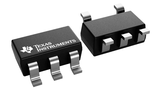
SN74LVC1G132 Series
Single 2-input, 1.65-V to 5.5-V NAND gate with Schmitt-Trigger inputs
Manufacturer: Texas Instruments
Catalog
Single 2-input, 1.65-V to 5.5-V NAND gate with Schmitt-Trigger inputs
Key Features
• Latch-Up Performance Exceeds 100 mA Per JESD 78, Class IIESD Protection Exceeds JESD 222000-V Human-Body Model (A114-A)200-V Machine Model (A115-A)1000-V Charged-Device Model (C101)Available in Texas InstrumentsNanoStar™ and NanoFree™ PackagesSupports 5-V VCCOperationInputs Accept Voltages to 5.5 VMax tpdof 5.3 ns at 3.3 VLow Power Consumption, 10-µA Maximum ICC±24-mA Output Drive at 3.3 VIoffSupports Partial-Power-Down Mode OperationLatch-Up Performance Exceeds 100 mA Per JESD 78, Class IIESD Protection Exceeds JESD 222000-V Human-Body Model (A114-A)200-V Machine Model (A115-A)1000-V Charged-Device Model (C101)Available in Texas InstrumentsNanoStar™ and NanoFree™ PackagesSupports 5-V VCCOperationInputs Accept Voltages to 5.5 VMax tpdof 5.3 ns at 3.3 VLow Power Consumption, 10-µA Maximum ICC±24-mA Output Drive at 3.3 VIoffSupports Partial-Power-Down Mode Operation
Description
AI
The SN74LVC1G132 device contains one 2-input NAND gate with Schmitt-trigger inputs designed for 1.65-V to 5.5-V VCCoperation and performs the Boolean function Y =A × Bor Y =A+Bin positive logic.
Because of Schmitt action, this device has different input threshold levels for positive-going (VT+) and negative-going (VT–) signals.
This device can be triggered from the slowest of input ramps and still give clean jitter-free output signals.
This device is fully specified for partial-power-down applications using Ioff. The Ioffcircuitry disables the outputs, preventing damaging current backflow through the device when it is powered down.
NanoStar™ and NanoFree™ package technology is a major breakthrough in IC packaging concepts, using the die as the package.


