SN74ALVC164245 Series
16-Bit 2.5-V to 3.3-V/3.3-V To 5-V Level Shifting Transceiver With 3-State Outputs
Manufacturer: Texas Instruments
Catalog
16-Bit 2.5-V to 3.3-V/3.3-V To 5-V Level Shifting Transceiver With 3-State Outputs
Key Features
• Member of the Texas Instruments Widebus™ FamilyMaximum tpdof 5.8 ns at 3.3 V±24-mA Output Drive at 3.3 VControl Inputs VIH/VILLevels Are Referenced to VCCAVoltageLatch-Up Performance Exceeds 250 mA Per JESD 17APPLICATIONSElectronic Points of SalePrinters and Other PeripheralsMotor DrivesWireless and Telecom InfrastructuresWearable Health and Fitness DevicesAll other trademarks are the property of their respective ownersMember of the Texas Instruments Widebus™ FamilyMaximum tpdof 5.8 ns at 3.3 V±24-mA Output Drive at 3.3 VControl Inputs VIH/VILLevels Are Referenced to VCCAVoltageLatch-Up Performance Exceeds 250 mA Per JESD 17APPLICATIONSElectronic Points of SalePrinters and Other PeripheralsMotor DrivesWireless and Telecom InfrastructuresWearable Health and Fitness DevicesAll other trademarks are the property of their respective owners
Description
AI
This 16-bit (dual-octal) noninverting bus transceiver contains two separate supply rails. B port has VCCB, which is set to operate at 3.3 V and 5 V. A port has VCCA, which is set to operate at 2.5 V and 3.3 V. This allows for translation from a 2.5-V to a 3.3-V environment, and vice versa, or from a 3.3-V to a 5-V environment, and vice versa.
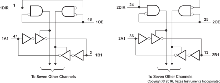
The SN74ALVC164245 is designed for asynchronous communication between data buses. The control circuitry (1DIR, 2DIR, 1OE, and 2OE) is powered by VCCA.
To ensure the high-impedance state during power up or power down, the output-enable (OE) input should be tied to VCCthrough a pullup resistor; the minimum value of the resistor is determined by the current-sinking capability of the driver.
The logic levels of the direction-control (DIR) input and the output-enable (OE) input activate either the B-port outputs or the A-port outputs or place both output ports into the high-impedance mode. The device transmits data from the A bus to the B bus when the B-port outputs are activated, and from the B bus to the A bus when the A-port outputs are activated. The input circuitry on both A and B ports always is active and must have a logic HIGH or LOW level applied to prevent excess ICCand ICCZ.


