Catalog
Single-bit dual-supply bus transceiver
Key Features
• Fully Configurable Dual-Rail Design Allows Each Port to Operate With a Power Supply Range from 0.65 V to 3.6 VOperating Temperature: –40°C to +125°CGlitch-Free Power Supply SequencingBus-hold on Data Inputs Eliminates the Need for External Pullup or Pulldown ResistorsMaximum Quiescent Current (ICCA+ ICCB) of 10 µA (85°C Maximum) and 16 µA (125°C Maximum)Up to 500-Mbps Support When Translating from 1.8 to 3.3 VVCCIsolation FeatureIf Either VCCInput is Below 100 mV, All I/Os Outputs are Disabled and Become High-ImpedanceIoffSupports Partial-Power-Down Mode OperationLatch-Up Performance Exceeds 100 mA Per JESD 78, Class IIESD Protection Exceeds JESD 228000-V Human Body Model1000-V Charged-Device ModelFully Configurable Dual-Rail Design Allows Each Port to Operate With a Power Supply Range from 0.65 V to 3.6 VOperating Temperature: –40°C to +125°CGlitch-Free Power Supply SequencingBus-hold on Data Inputs Eliminates the Need for External Pullup or Pulldown ResistorsMaximum Quiescent Current (ICCA+ ICCB) of 10 µA (85°C Maximum) and 16 µA (125°C Maximum)Up to 500-Mbps Support When Translating from 1.8 to 3.3 VVCCIsolation FeatureIf Either VCCInput is Below 100 mV, All I/Os Outputs are Disabled and Become High-ImpedanceIoffSupports Partial-Power-Down Mode OperationLatch-Up Performance Exceeds 100 mA Per JESD 78, Class IIESD Protection Exceeds JESD 228000-V Human Body Model1000-V Charged-Device Model
Description
AI
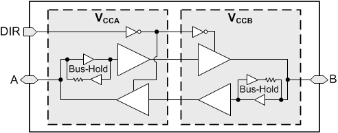
The SN74AXCH1T45 is a single-bit noninverting bus transceiver that uses two individually configurable power-supply rails. The device is operational with both VCCAand VCCBsupplies as low as 0.65 V. The A port is designed to track VCCA, which accepts any supply voltage from 0.65 V to 3.6 V. The B port is designed to track VCCB, which also accepts any supply voltage from 0.65 V to 3.6 V. Additionally the SN74AXCH1T45 is compatible with a single-supply system.
The DIR pin determines the direction of signal propagation. With the DIR pin configured HIGH, translation is from Port A to Port B. With DIR configured LOW, translation is from Port B to Port A. The DIR pin is referenced to VCCA, meaning that its logic-high and logic-low thresholds track with VCCA.
Active bus-hold circuitry holds unused or undriven inputs at a valid logic state. Use of pullup or pulldown resistors with the bus-hold circuitry is not recommended. If a supply is present for VCCAor VCCB, the bus-hold circuitry always remains active on the A or B inputs respectively, independent of the state of the direction control pin.
This device is fully specified for partial-power-down applications using the Ioffcurrent. The Ioffprotection circuitry ensures that no excessive current is drawn from or to an input, output, or combined I/O that is biased to a specific voltage while the device is powered down.
The VCCisolation feature ensures that if either VCCAor VCCBis less than 100 mV, both I/O ports enter a high-impedance state by disabling their outputs.
Glitch-free power supply sequencing allows either supply rail to be powered on or off in any order while providing robust power sequencing performance.


