ADC3660 Series
Dual, 16-bit, 0.5-MSPS to 65-MSPS, low-noise, ultra-low-power analog-to-digital converter (ADC)
Manufacturer: Texas Instruments
Catalog
Dual, 16-bit, 0.5-MSPS to 65-MSPS, low-noise, ultra-low-power analog-to-digital converter (ADC)
Key Features
• Dual channel16-bit 65 MSPS ADC (max output rate = 31 Msps)Noise floor: –159 dBFS/HzUltra-low power: 71 mW/ch at 65 MSPS16-Bit, no missing codesINL: ±2 LSB; DNL: ±0.2 LSBReference: external or internalInput bandwidth: 900 MHz (3 dB)Industrial temperature range: –40°C to +105°COn-chip digital down converterDecimation by 2, 4, 8, 16, 3232-bit NCOSerial CMOS interfaceSingle 1.8-V supplySmall footprint: 40-WQFN (5 mm × 5 mm) packageSpectral performance (fIN= 5 MHz):SNR: 81.9 dBFSSFDR: 88 dBc HD2, HD3SFDR: 102 dBFS worst spurDual channel16-bit 65 MSPS ADC (max output rate = 31 Msps)Noise floor: –159 dBFS/HzUltra-low power: 71 mW/ch at 65 MSPS16-Bit, no missing codesINL: ±2 LSB; DNL: ±0.2 LSBReference: external or internalInput bandwidth: 900 MHz (3 dB)Industrial temperature range: –40°C to +105°COn-chip digital down converterDecimation by 2, 4, 8, 16, 3232-bit NCOSerial CMOS interfaceSingle 1.8-V supplySmall footprint: 40-WQFN (5 mm × 5 mm) packageSpectral performance (fIN= 5 MHz):SNR: 81.9 dBFSSFDR: 88 dBc HD2, HD3SFDR: 102 dBFS worst spur
Description
AI
The ADC3660 device is a low-noise, ultra-low power, 16-bit, 65-MSPS dual-channel, high-speed analog-to-digital converter (ADCs). Designed for low power consumption, the device delivers a noise spectral density of –159 dBFS/Hz, combined with excellent linearity and dynamic range. The ADC3660 offers excellent dc precision, together with IF sampling support, which make the device an excellent choice for a wide range of applications. The ADC consumes only 71 mW/ch at 65 MSPS, and power consumption scales very well with lower sampling rates. In bypass mode (up to 31 MSPS) the output data is available after 1 or 2 clock cycles.
The ADC3660 uses a serial CMOS (SCMOS) interface to output the data which minimizes the number of digital interconnects. The device supports a two-lane, a one-lane and a half lane option. The serialized CMOS interface supports output rates to 250 Mbps which translates to ~ 15 MSPS (2-wire) to ~ 3.75 MSPS (0.5-wire) output rates after complex decimation. Hence the ADC3660 can be operated in ’oversampling + decimating’ mode using the internal decimation filter in order to improve the dynamic range and relax external anti-aliasing filter.
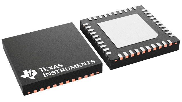
The device comes in a 40-pin WQFN package (5 mm × 5 mm) and supports the extended industrial temperature range of –40 to +105⁰C.


