SN74ABT16241A Series
16-ch, 4.5-V to 5.5-V buffers with TTL-compatible CMOS inputs and 3-state outputs
Manufacturer: Texas Instruments
Catalog
16-ch, 4.5-V to 5.5-V buffers with TTL-compatible CMOS inputs and 3-state outputs
Key Features
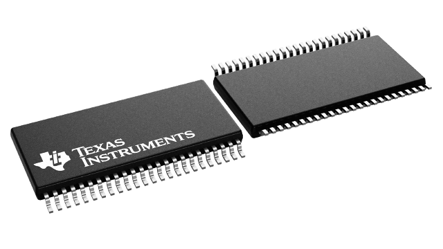
• Members of the Texas InstrumentsWidebusTMFamilyState-of-the-ArtEPIC-IIBTMBiCMOS Design Significantly Reduces Power DissipationTypical VOLP(Output Ground Bounce) < 1 V at VCC= 5 V, TA= 25°CDistributed VCCand GND Pin Configuration Minimizes High-Speed Switching NoiseFlow-Through Architecture Optimizes PCB LayoutHigh-Drive Outputs (-32-mA IOH, 64-mA IOL)Latch-Up Performance Exceeds 500 mAPer JESD 17ESD Protection Exceeds 2000 V Per MIL-STD-883, Method 3015; Exceeds 200 V Using Machine Model (C = 200 pF, R = 0)Package Options Include Plastic 300-mil Shrink Small-Outline (DL), Thin Shrink Small-Outline (DGG), and Thin Very Small-Outline (DGV) Packages and 380-mil Fine-Pitch Ceramic Flat (WD) Package Using 25-mil Center-to-Center SpacingsWidebus and EPIC-IIB are trademarks of Texas Instruments Incorporated.Members of the Texas InstrumentsWidebusTMFamilyState-of-the-ArtEPIC-IIBTMBiCMOS Design Significantly Reduces Power DissipationTypical VOLP(Output Ground Bounce) < 1 V at VCC= 5 V, TA= 25°CDistributed VCCand GND Pin Configuration Minimizes High-Speed Switching NoiseFlow-Through Architecture Optimizes PCB LayoutHigh-Drive Outputs (-32-mA IOH, 64-mA IOL)Latch-Up Performance Exceeds 500 mAPer JESD 17ESD Protection Exceeds 2000 V Per MIL-STD-883, Method 3015; Exceeds 200 V Using Machine Model (C = 200 pF, R = 0)Package Options Include Plastic 300-mil Shrink Small-Outline (DL), Thin Shrink Small-Outline (DGG), and Thin Very Small-Outline (DGV) Packages and 380-mil Fine-Pitch Ceramic Flat (WD) Package Using 25-mil Center-to-Center SpacingsWidebus and EPIC-IIB are trademarks of Texas Instruments Incorporated.
Description
AI
The 'ABT16241A devices are 16-bit buffers and line drivers designed specifically to improve both the performance and density of 3-state memory address drivers, clock drivers, and bus-oriented receivers and transmitters.
These devices can be used as four 4-bit buffers, two 8-bit buffers, or one 16-bit buffer. These devices provide true outputs and complementary output-enable (OE and OE\) inputs.
To ensure the high-impedance state during power up or power down, OE\ should be tied to VCCthrough a pullup resistor; the minimum value of the resistor is determined by the current-sinking capability of the driver. OE should be tied to GND through a pulldown resistor; the minimum value of the resistor is determined by the current-sourcing capability of the driver.
The SN54ABT16241A is characterized for operation over the full military temperature range of -55°C to 125°C. The SN74ABT16241A is characterized for operation from -40°C to 85°C.


