TLC1550 Series
10-Bit, 164 kSPS ADC Parallel Out, Direct I/F to DSP/uProcessor
Manufacturer: Texas Instruments
Catalog
10-Bit, 164 kSPS ADC Parallel Out, Direct I/F to DSP/uProcessor
Key Features
• Power Dissipation...40 mW MaxAdvanced LinEPIC™ Single-Poly Process Provides Close Capacitor Matching for Better AccuracyFast Parallel Processing for DSP and µP InterfaceEither External or Internal Clock Can Be UsedConversion Time...6 µsTotal Unadjusted Error...±1 LSB MaxCMOS TechnologyAdvanced LinEPIC is a trademark of Texas Instruments.Power Dissipation...40 mW MaxAdvanced LinEPIC™ Single-Poly Process Provides Close Capacitor Matching for Better AccuracyFast Parallel Processing for DSP and µP InterfaceEither External or Internal Clock Can Be UsedConversion Time...6 µsTotal Unadjusted Error...±1 LSB MaxCMOS TechnologyAdvanced LinEPIC is a trademark of Texas Instruments.
Description
AI
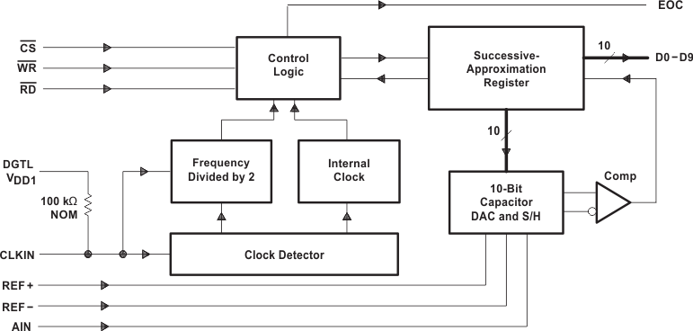
The TLC1550x and TLC1551 are data acquisition analog-to-digital converters (ADCs) using a 10-bit, switched-capacitor, successive-approximation network. A high-speed, 3-state parallel port directly interfaces to a digital signal processor (DSP) or microprocessor (µP) system data bus. D0 through D9 are the digital output terminals with D0 being the least significant bit (LSB). Separate power terminals for the analog and digital portions minimize noise pickup in the supply leads. Additionally, the digital power is divided into two parts to separate the lower current logic from the higher current bus drivers. An external clock can be applied to CLKIN to override the internal system clock if desired.
The TLC1550I and TLC1551I are characterized for operation from –40°C to 85°C. The TLC1550M is characterized over the full military range of –55°C to 125°C.


