ADC09QJ800-Q1 Series
Automotive quad-channel, 9-bit, 800-MSPS analog-to-digital converter (ADC) with JESD204C interface
Manufacturer: Texas Instruments
Catalog
Automotive quad-channel, 9-bit, 800-MSPS analog-to-digital converter (ADC) with JESD204C interface
Key Features
• AEC-Q100 qualified for automotive applications:Temperature grade 1: –40°C to +125°C, TAADC Core:Resolution: 9 BitNon-interleaved architectureInternal dither reduces high-order harmonicsPerformance specifications:SNR (–1dBFS, 97MHz): 53.5dBFSENOB (–1dBFS, 97MHz): 8.51 BitsSFDR (–1dBFS, 97MHz): 64dBFSNoise floor (–20dBFS, 97MHz): –140.5dBFS/HzFull-scale input voltage: 800mVPP-DIFFFull-power input bandwidth: 6GHzJESD204C Serial data interface:Support for 2 to 8 (Quad/Dual channel) or 1 to 4 (Single channel) total SerDes lanesMaximum baud-rate: 17.16Gbps64B/66B and 8B/10B encoding modesSubclass-1 support for deterministic latencyCompatible with JESD204B receiversOptional internal sampling clock generationInternal PLL and VCO (7.2–8.2GHz)SYSREF Windowing eases synchronizationFour clock outputs simplify system clockingReference clocks for FPGA or adjacent ADCReference clock for SerDes transceiversTimestamp input and output for pulsed systemsPower consumption (800MSPS):Quad Channel: 420mW / channelDual channel: 555mW / channelSingle channel: 840mWPower supplies: 1.1V, 1.9VAEC-Q100 qualified for automotive applications:Temperature grade 1: –40°C to +125°C, TAADC Core:Resolution: 9 BitNon-interleaved architectureInternal dither reduces high-order harmonicsPerformance specifications:SNR (–1dBFS, 97MHz): 53.5dBFSENOB (–1dBFS, 97MHz): 8.51 BitsSFDR (–1dBFS, 97MHz): 64dBFSNoise floor (–20dBFS, 97MHz): –140.5dBFS/HzFull-scale input voltage: 800mVPP-DIFFFull-power input bandwidth: 6GHzJESD204C Serial data interface:Support for 2 to 8 (Quad/Dual channel) or 1 to 4 (Single channel) total SerDes lanesMaximum baud-rate: 17.16Gbps64B/66B and 8B/10B encoding modesSubclass-1 support for deterministic latencyCompatible with JESD204B receiversOptional internal sampling clock generationInternal PLL and VCO (7.2–8.2GHz)SYSREF Windowing eases synchronizationFour clock outputs simplify system clockingReference clocks for FPGA or adjacent ADCReference clock for SerDes transceiversTimestamp input and output for pulsed systemsPower consumption (800MSPS):Quad Channel: 420mW / channelDual channel: 555mW / channelSingle channel: 840mWPower supplies: 1.1V, 1.9V
Description
AI
ADC09xJ800-Q1 is a family of quad, dual and single channel, 9-bit, 800MSPS analog-to-digital converters (ADC). Low power consumption, high sampling rate and 9-bit resolution makes the ADC09xJ800-Q1 suited for light detection and ranging (LiDAR) systems. The ADC09xJ800-Q1 is qualified for automotive applications.
Full-power input bandwidth (-3dB) of 6GHz provides flat frequency response for frequency modulated continuous wave (FMCW) LiDAR systems and provides a narrow impulse response for pulse-based systems. The full-power input bandwidth also enables direct RF sampling of up to 4GHz.
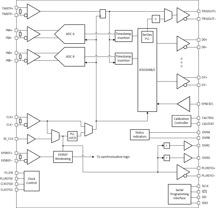
A number of clocking features are included to relax system hardware requirements, such as an internal phase-locked loop (PLL) with integrated voltage-controlled oscillator (VCO) to generate the sampling clock. Four clock outputs are provided to clock the logic and SerDes of the FPGA or ASIC. A timestamp input and output is provided for pulsed systems.
JESD204C serialized interface decreases system size by reducing the amount of printed circuit board (PCB) routing. Interface modes support from 2 to 8 lanes (dual and quad channel devices) or 1 to 4 lanes (for the single channel device), with SerDes baud-rates up to 17.16Gbps, to allow the optimal configuration for each application.


