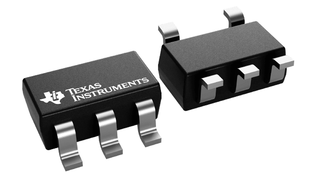
TPS2819-Q1 Series
Enhanced Product 2-A/2-A single-channel gate driver wih 40-V VDD and regulated output
Manufacturer: Texas Instruments
Catalog
Enhanced Product 2-A/2-A single-channel gate driver wih 40-V VDD and regulated output
Key Features
• Controlled BaselineOne Assembly SiteOne Test SiteOne Fabrication SiteExtended Temperature Performance of -55°C to 125°CEnhanced Diminishing Manufacturing Sources (DMS) SupportEnhanced Product-Change NotificationQualification Pedigree(1)Low-Cost Single-Channel High-Speed MOSFET DriverICC. . . 15-µA Max (TPS2828, TPS2829)25 ns Max Rise/Fall Times and 40 ns Max Propagation Delay . . . 1 nF Load2-A Peak Output Current4 V to 14 V Driver Supply Voltage Range; Internal Regulator Extends Range to 40 V (TPS2816, TPS2817, TPS2818, TPS2819)5-pin SOT-23 Package-55°C to 125°C Ambient-Temperature Operating RangeHighly Resistant to Latch-ups(1)Component qualification in accordance with JEDEC and industry standards to ensure reliable operation over an extended temperature range. This includes, but is not limited to, Highly Accelerated Stress Test (HAST) or biased 85/85, temperature cycle, autoclave or unbiased HAST, electromigration, bond intermetallic life, and mold compound life. Such qualification testing should not be viewed as justifying use of this component beyond specified performance and environmental limitsControlled BaselineOne Assembly SiteOne Test SiteOne Fabrication SiteExtended Temperature Performance of -55°C to 125°CEnhanced Diminishing Manufacturing Sources (DMS) SupportEnhanced Product-Change NotificationQualification Pedigree(1)Low-Cost Single-Channel High-Speed MOSFET DriverICC. . . 15-µA Max (TPS2828, TPS2829)25 ns Max Rise/Fall Times and 40 ns Max Propagation Delay . . . 1 nF Load2-A Peak Output Current4 V to 14 V Driver Supply Voltage Range; Internal Regulator Extends Range to 40 V (TPS2816, TPS2817, TPS2818, TPS2819)5-pin SOT-23 Package-55°C to 125°C Ambient-Temperature Operating RangeHighly Resistant to Latch-ups(1)Component qualification in accordance with JEDEC and industry standards to ensure reliable operation over an extended temperature range. This includes, but is not limited to, Highly Accelerated Stress Test (HAST) or biased 85/85, temperature cycle, autoclave or unbiased HAST, electromigration, bond intermetallic life, and mold compound life. Such qualification testing should not be viewed as justifying use of this component beyond specified performance and environmental limits
Description
AI
The TPS28xx single-channel high-speed MOSFET drivers are capable of delivering peak currents of up to 2 A into highly capacitive loads. High switching speeds (trand tf= 14 ns typ) are obtained with the use of BiCMOS outputs. Typical threshold switching voltages are two-thirds and one-third of VCC. The design inherently minimizes shoot-through current.
A regulator is provided on TPS2816 through TPS2819 devices to allow operation with supply inputs between 14V and 40V. The regulator output can be used to power other circuits, provided power dissipation does not exceed package limitations. If the regulator is not required, VDD(the regulator input) should be connected to VCC. The TPS2816 and TPS2817 input circuits include an active pullup circuit to eliminate the need for an external resistor when using open-collector PWM controllers. The TPS2818 and TPS2819 are identical to the TPS2816 and TPS2817, except that the active pullup circuit is omitted. The TPS2828 and TPS2829 are identical to the TPS2818 and TPS2819, except that the internal voltage regulator is omitted, allowing quiescent current to drop to less than 15 µA when the inputs are high or low.
The TPS28xx series devices are available in 5-pin SOT-23 (DBV) packages and operate over an ambient temperature range of –40°C to 125°C.


