Catalog
Automotive 3.125-Gbps LVDS 2x2 crosspoint switch
Key Features
• AECQ-100 Grade 3DC - 3.125 Gbps Low Jitter, Low Skew, Low Power OperationPin Configurable, Fully Differential, Non-Blocking ArchitectureOn-chip 100Ω Input and Output Terminations Minimize Return Losses, Reduce Component Count and Minimize Board Space8 kV ESD on LVDS I/O Pins Protects Adjoining ComponentsSmall 4 mm x 4 mm WQFN-16 Space Saving PackageAECQ-100 Grade 3DC - 3.125 Gbps Low Jitter, Low Skew, Low Power OperationPin Configurable, Fully Differential, Non-Blocking ArchitectureOn-chip 100Ω Input and Output Terminations Minimize Return Losses, Reduce Component Count and Minimize Board Space8 kV ESD on LVDS I/O Pins Protects Adjoining ComponentsSmall 4 mm x 4 mm WQFN-16 Space Saving Package
Description
AI
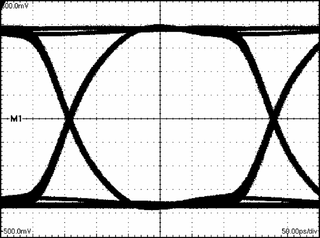
The DS25CP152Q is a 3.125 Gbps 2x2 LVDS crosspoint switch optimized for high-speed signal routing and switching over lossy FR-4 printed circuit board backplanes and balanced cables. Fully differential signal paths ensure exceptional signal integrity and noise immunity. The non-blocking architecture allows connections of any input to any output or outputs.
Wide input common mode range allows the switch to accept signals with LVDS, CML and LVPECL levels; the output levels are LVDS. A very small package footprint requires a minimal space on the board while the flow-through pinout allows easy board layout. Each differential input and output is internally terminated with a 100Ω resistor to lower device return losses, reduce component count and further minimize board space.


