Catalog
12-V, 1:1 (SPST), (SPST), 4-channel analog switch
Key Features
• Wide analog-input-voltage range: 0 V – 10 VLow ON resistance:VCC = 4.5 V: 25 ΩVCC = 9 V: 15 ΩFast switching and propagation delay timesLow OFF leakage currentWide operating temperature range: –55°C to 125°CHC types:2 V to 10 V operationHigh noise immunity: NIL = 30%, NIH = 30% of VCC at VCC = 5 V and 10 VHCT types:Direct LSTTL input logic compatibility, VIL= 0.8 V (maximum), VIH = 2 V (minimum)CMOS input compatibility, Il ≤ 1 µA at VOL, VOHWide analog-input-voltage range: 0 V – 10 VLow ON resistance:VCC = 4.5 V: 25 ΩVCC = 9 V: 15 ΩFast switching and propagation delay timesLow OFF leakage currentWide operating temperature range: –55°C to 125°CHC types:2 V to 10 V operationHigh noise immunity: NIL = 30%, NIH = 30% of VCC at VCC = 5 V and 10 VHCT types:Direct LSTTL input logic compatibility, VIL= 0.8 V (maximum), VIH = 2 V (minimum)CMOS input compatibility, Il ≤ 1 µA at VOL, VOH
Description
AI
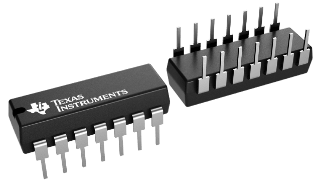
The SN74HC4066 device is a silicon-gate CMOS quadruple analog switch designed to handle both analog and digital signals. Each switch permits signals with amplitudes of up to 6V (peak) to be transmitted in either direction.
Each switch section has its own enable input control (C). A high-level voltage applied to C turns on the associated switch section.
Applications include signal gating, chopping, modulation or demodulation (modem), and signal multiplexing for analog-to-digital and digital-to-analog conversion systems.


