SN74AXC4T245-Q1 Series
Automotive 4-bit dual-supply bus transceiver w/ configurable voltage translation, 3-state output
Manufacturer: Texas Instruments
Catalog
Automotive 4-bit dual-supply bus transceiver w/ configurable voltage translation, 3-state output
Key Features
• AEC-Q100 qualified for automotive applicationsAvailable in wettable flank QFN (WBQB) packageFully-configurable dual-rail design allows each port to operate with a power supply range from 0.65V to 3.6VOperating temperature from –40°C to +125°CMultiple direction control pins to allow simultaneous up and down translationGlitch-free power supply sequencingUp to 380 Mbps support when translating from 1.8V to 3.3VVCC isolation feature:If either VCC input is below 100mV, all I/O outputs are disabled and become high impedanceIoff supports partial-power-down mode operationCompatible with AVC-family level shiftersLatch-up performance exceeds 100mA per JESD 78, class IIESD protection exceeds JEDEC JS-0018000V human-body model1000V charged-device modelAEC-Q100 qualified for automotive applicationsAvailable in wettable flank QFN (WBQB) packageFully-configurable dual-rail design allows each port to operate with a power supply range from 0.65V to 3.6VOperating temperature from –40°C to +125°CMultiple direction control pins to allow simultaneous up and down translationGlitch-free power supply sequencingUp to 380 Mbps support when translating from 1.8V to 3.3VVCC isolation feature:If either VCC input is below 100mV, all I/O outputs are disabled and become high impedanceIoff supports partial-power-down mode operationCompatible with AVC-family level shiftersLatch-up performance exceeds 100mA per JESD 78, class IIESD protection exceeds JEDEC JS-0018000V human-body model1000V charged-device model
Description
AI
The SN74AXC4T245-Q1 AEC-Q100 qualified device is a four-bit non-inverting bus transceiver that uses two individually configurable power-supply rails. The device is operational with both VCCA and VCCB supplies as low as 0.65V. The A port is designed to track VCCA, which accepts any supply voltage from 0.65V to 3.6V. The B port is designed to track VCCB, which also accepts any supply voltage from 0.65V to 3.6V. Additionally the SN74AXC4T245-Q1 is compatible with a single-supply system.
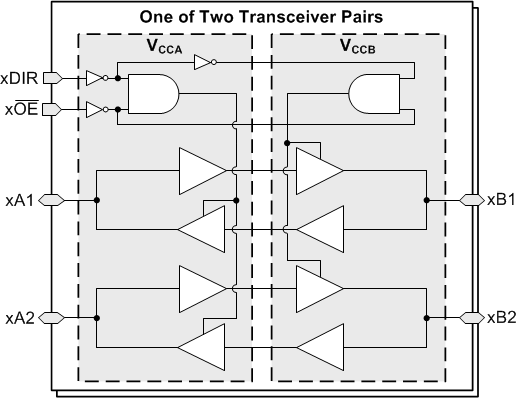
The SN74AXC4T245-Q1 device is designed for asynchronous communication between data buses. The device transmits data from the A bus to the B bus or from the B bus to the A bus, depending on the logic level of the direction-control inputs (1DIR and 2DIR). The output-enable inputs (1 OE and 2 OE) are used to disable the outputs so the buses are effectively isolated. The SN74AXC4T245-Q1 device is designed so the control pins (xDIR and x OE) are referenced to VCCA.
To put the level shifter I/Os in the high-impedance state during power up or power down, tie the x OE pins to VCCA through a pull-up resistor.
This device is fully specified for partial-power-down applications using the Ioff current. The Ioff protection circuitry is designed so that no excessive current is drawn from or to an input, output, or combined I/O that is biased to a specific voltage while the device is powered down.
The VCC isolation feature is designed so that if either VCCA or VCCB is less than 100mV, both I/O ports enter a high-impedance state by disabling their outputs.
Glitch-Free power supply sequencing allows either supply rail to be powered on or off in any order while providing robust power sequencing performance.


