TPS54116-Q1 Series
Automotive DDR Power Solution with 4-A, 2-MHz VDDQ DC/DC Converter, 1-A VTT LDO and VTTREF
Manufacturer: Texas Instruments
Catalog
Automotive DDR Power Solution with 4-A, 2-MHz VDDQ DC/DC Converter, 1-A VTT LDO and VTTREF
Key Features
• AEC-Q100 Qualified With the Following Results:Device Temperature Grade 1: –40°C to +125°C Ambient Operating Temperature RangeDevice HBM ESD Classification Level 2Device CDM ESD Classification Level C6Single-chip DDR2, DDR3 and DDR3L Memory Power Solution4-A Synchronous Buck ConverterIntegrated 33-mΩ High-side and 25-mΩ Low-side MOSFETsFixed Frequency Current-mode ControlAdjustable Frequency from 100 kHz to 2.5 MHzSynchronizable to an External Clock0.6-V ±1% Voltage Reference Over TemperatureAdjustable Cycle-by-Cycle Peak Current LimitMonotonic Start-up Into Pre-biased Outputs1-A Source/Sink Termination LDO with ±20-mV DC AccuracyStable with 2 × 10-µF MLCC Capacitor10-mA Source/Sink Buffered Reference Output Regulated to Within 49% to 51% of VDDQIndependent Enable Pins with Adjustable UVLO and HysteresisThermal Shutdown–40°C to 150°C Operating TJ24-pin, 4-mm × 4-mm WQFN PackageAEC-Q100 Qualified With the Following Results:Device Temperature Grade 1: –40°C to +125°C Ambient Operating Temperature RangeDevice HBM ESD Classification Level 2Device CDM ESD Classification Level C6Single-chip DDR2, DDR3 and DDR3L Memory Power Solution4-A Synchronous Buck ConverterIntegrated 33-mΩ High-side and 25-mΩ Low-side MOSFETsFixed Frequency Current-mode ControlAdjustable Frequency from 100 kHz to 2.5 MHzSynchronizable to an External Clock0.6-V ±1% Voltage Reference Over TemperatureAdjustable Cycle-by-Cycle Peak Current LimitMonotonic Start-up Into Pre-biased Outputs1-A Source/Sink Termination LDO with ±20-mV DC AccuracyStable with 2 × 10-µF MLCC Capacitor10-mA Source/Sink Buffered Reference Output Regulated to Within 49% to 51% of VDDQIndependent Enable Pins with Adjustable UVLO and HysteresisThermal Shutdown–40°C to 150°C Operating TJ24-pin, 4-mm × 4-mm WQFN Package
Description
AI
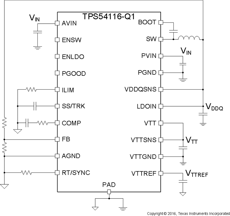
The TPS54116-Q1 device is a full featured 6-V, 4-A, synchronous step down converter with two integrated MOSFETs and 1-A sink/source double data rate (DDR) VTT termination regulator with VTTREF buffered reference output.
The TPS54116-Q1 buck regulator minimizes solution size by integrating the MOSFETs and reducing inductor size with up to 2.5-MHz switching frequency. The switching frequency can be set above the medium wave radio band for noise sensitive applications and is synchronizable to an external clock. Synchronous rectification keeps the frequency fixed across the entire output load range. Efficiency is maximized through integrated 25-mΩ low-side and 33-mΩ high-side MOSFETs. Cycle-by-cycle peak current limit protects the device during an overcurrent condition and is adjustable with a resistor at the ILIM pin to optimize for smaller inductors.
The VTT termination regulator maintains fast transient response with only 2 × 10-µF ceramic output capacitance reducing external component count. The TPS54116-Q1 uses remote sensing of VTT for best regulation.
Using the enable pins to enter a shutdown mode reduces supply current to 1-µA. Under voltage lockout thresholds can be set with a resistor network on either enable pin. The VTT and VTTREF outputs are discharged when disabled with ENLDO.
Full integration minimizes the IC footprint with a small 4 mm × 4 mm thermally enhanced WQFN package.


