DAC7551-Q1 Series
Automotive 12-Bit, Ultralow Glitch, Voltage Output Digital to Analog Converter
Manufacturer: Texas Instruments
Catalog
Automotive 12-Bit, Ultralow Glitch, Voltage Output Digital to Analog Converter
Key Features
• Qualified for Automotive ApplicationsRelative Accuracy (INL): ±0.35 LSBUltra-Low Glitch Energy: 0.1 nV-sLow-Power Operation: 100 µA at 2.7 VPower-On Reset-to-Zero ScalePower Supply: 2.7- to 5.5-V Single SupplyPower-Down: 0.05 µA at 2.7 V12-Bit Linearity and MonotonicityRail-to-Rail Voltage OutputSettling Time: 5 µs (Max)SPI-Compatible Serial Interface With Schmitt-Trigger Input: Up to 50 MHzDaisy-Chain CapabilityAsynchronous Hardware Clear-to-Zero ScaleSpecified Temperature Range:–40°C to +105°CSmall, 2-mm × 3-mm, 12-Lead USON PackageZ-Suffix Offers Improved DelaminationQualified for Automotive ApplicationsRelative Accuracy (INL): ±0.35 LSBUltra-Low Glitch Energy: 0.1 nV-sLow-Power Operation: 100 µA at 2.7 VPower-On Reset-to-Zero ScalePower Supply: 2.7- to 5.5-V Single SupplyPower-Down: 0.05 µA at 2.7 V12-Bit Linearity and MonotonicityRail-to-Rail Voltage OutputSettling Time: 5 µs (Max)SPI-Compatible Serial Interface With Schmitt-Trigger Input: Up to 50 MHzDaisy-Chain CapabilityAsynchronous Hardware Clear-to-Zero ScaleSpecified Temperature Range:–40°C to +105°CSmall, 2-mm × 3-mm, 12-Lead USON PackageZ-Suffix Offers Improved Delamination
Description
AI
The DAC7551-Q1 device is a single-channel, voltage-output digital-to-analog converter (DAC) with exceptional linearity and monotonicity, and a proprietary architecture that minimizes glitch energy. The low-power DAC7551-Q1 device operates from a single 2.7- to 5.5-V supply. The DAC7551-Q1 output amplifiers can drive a 2-kΩ, 200-pF load rail-to-rail with 5-µs settling time. The output range is set using an external voltage reference.
The 3-wire serial interface operates at clock rates up to 50 MHz and is compatible with SPI™, QSPI™, microwire, and DSP interface standards. The device incorporates a power-on-reset (POR) circuit to ensure that the DAC output powers up to 0 V and remains at that voltage until a valid write cycle to the device occurs. The device contains a power-down feature that reduces the current consumption of the device to under 2 µA.
Small size and low-power operation make the DAC7551-Q1 device ideally suited for battery-operated, portable applications. The power consumption is typically 0.5 mW at 5 V, 0.23 mW at 3 V, and reduces to 1 µW in power-down mode.
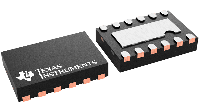
The DAC7551-Q1 device is available in a 12-pin USON package and is specified over –40°C to +105°C. The Z-suffix offers reduced delamination compared to standard device.


