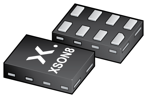
74LVC2T45GS Series
Dual supply translating transceiver; 3-state
Manufacturer: Freescale Semiconductor - NXP
Catalog
Dual supply translating transceiver; 3-state
Key Features
• Wide supply voltage range:
• VCC(A): 1.2 V to 5.5 V
• VCC(B): 1.2 V to 5.5 V
• High noise immunity
• Complies with JEDEC standards:
• JESD8-7 (1.2 V to 1.95 V)
• JESD8-5 (1.8 V to 2.7 V)
• JESD8C (2.7 V to 3.6 V)
• JESD36 (4.5 V to 5.5 V)
• Maximum data rates:
• 420 Mbps (3.3 V to 5.0 V translation)
• 210 Mbps (translate to 3.3 V))
• 140 Mbps (translate to 2.5 V)
• 75 Mbps (translate to 1.8 V)
• 60 Mbps (translate to 1.5 V)
• Suspend mode
• Latch-up performance exceeds 100 mA per JESD 78 Class II
• ±24 mA output drive (VCC= 3.0 V)
• Inputs accept voltages up to 5.5 V
• Low power consumption: 16 μA maximum ICC
• IOFFcircuitry provides partial Power-down mode operation
• ESD protection:
• HBM: ANSI/ESDA/JEDEC JS-001 class 3A exceeds 4000 V
• CDM: ANSI/ESDA/JEDEC JS-002 class C3 exceeds 1000 V
• Multiple package options
• Specified from -40 °C to +85 °C and -40 °C to +125 °C
Description
AI
The 74LVC2T45; 74LVCH2T45 are dual bit, dual supply translating transceivers with 3-state outputs that enable bidirectional level translation. They feature two 2-bits input-output ports (nA and nB), a direction control input (DIR) and dual supply pins (VCC(A)and VCC(B)). Both VCC(A)and VCC(B)can be supplied at any voltage between 1.2 V and 5.5 V making the device suitable for translating between any of the low voltage nodes (1.2 V, 1.5 V, 1.8 V, 2.5 V, 3.3 V and 5.0 V). Pins nA and DIR are referenced to VCC(A)and pins nB are referenced to VCC(B). A HIGH on DIR allows transmission from nA to nB and a LOW on DIR allows transmission from nB to nA.


