Catalog
3.3-V or 5-V LVDS driver and receiver
Key Features
• LVDS Signaling3.3V or 5.0V operationLow power CMOS designBalanced Output ImpedanceGlitch free power up/down (Driver disabled)High Signaling Rate Capacity (above 100 Mbps)Ultra Low Power Dissipation±1V Common-Mode Range±100 mV Receiver SensitivityProduct offered in SOIC and TSSOP packagesFlow-Through Pin OutIndustrial Temperature Range OperationTRI-STATE® is a registered trademark of National Semiconductor Corporation.LVDS Signaling3.3V or 5.0V operationLow power CMOS designBalanced Output ImpedanceGlitch free power up/down (Driver disabled)High Signaling Rate Capacity (above 100 Mbps)Ultra Low Power Dissipation±1V Common-Mode Range±100 mV Receiver SensitivityProduct offered in SOIC and TSSOP packagesFlow-Through Pin OutIndustrial Temperature Range OperationTRI-STATE® is a registered trademark of National Semiconductor Corporation.
Description
AI
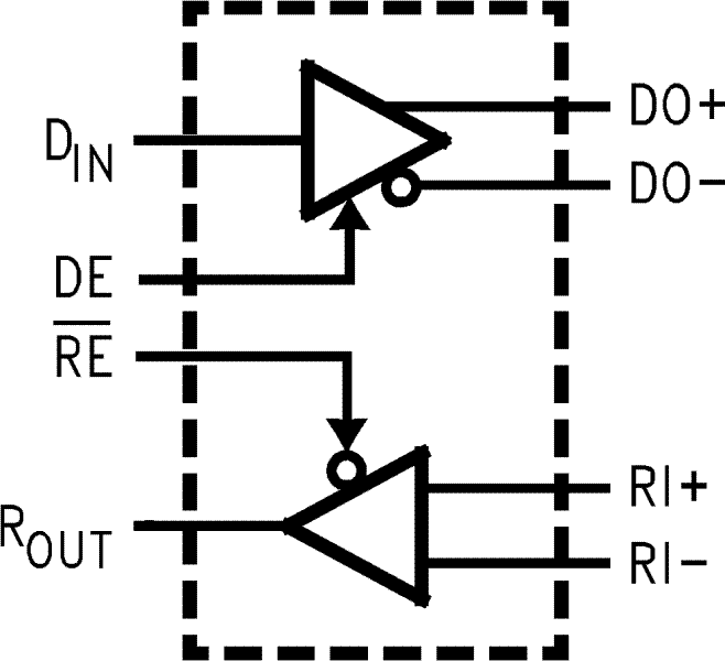
The DS90LV019 is a Driver/Receiver designed specifically for the high speed low power point-to-point interconnect applications. The device operates from a single 3.3V or 5.0V power supply and includes one differential line driver and one receiver. The DS90LV019 features an independent driver and receiver with TTL/CMOS compatibility (DINand ROUT). The logic interface provides maximum flexibility as 4 separate lines are provided (DIN, DE, RE#, and ROUT). The device also features a flow-through pin out which allows easy PCB routing for short stubs between its pins and the connector. The driver has 3.5 mA output loop current.
The driver translates between TTL levels (single-ended) to Low Voltage Differential Signaling levels. This allows for high speed operation, while consuming minimal power with reduced EMI. In addition, the differential signaling provides common-mode noise rejection.
The receiver threshold is ±100 mV over a ±1V common-mode range and translates the low swing differential levels to standard (TTL/CMOS) levels.


