CD4504B-EP Series
CMOS Hex Voltage-Level Shifter for TTL-to-CMOS or CMOS-to-CMOS Operation
Manufacturer: Texas Instruments
Catalog
CMOS Hex Voltage-Level Shifter for TTL-to-CMOS or CMOS-to-CMOS Operation
Key Features
• Independence of Power-Supply Sequence Considerations – VCCCan Exceed VDD;Input Signals Can Exceed Both VCCand VDDUp and Down Level-Shifting CapabilityShiftable Input Threshold for Either CMOS or TTL CompatibilityStandardized Symmetrical Output Characteristics100% Tested for Quiescent Current at 20 VMaximum Input Current of 1 µA at 18 V Over Full Package-Temperature Range:100 nA at 18 V and 25°C5 V, 10 V, and 15 V Parametric RatingsMeets All Requirements of JEDEC Standard No. 13B,"Standard Specifications for Description of ’B’ Series CMOS Devices"SUPPORTS DEFENSE, AEROSPACE, AND MEDICAL APPLICATIONSControlled BaselineOne Assembly/Test SiteOne Fabrication SiteAvailable in Military (–55°C/125°C) Temperature Range(1)Extended Product Life CycleExtended Product-Change NotificationProduct Traceability(1)Additional temperature ranges are available – contact factoryIndependence of Power-Supply Sequence Considerations – VCCCan Exceed VDD;Input Signals Can Exceed Both VCCand VDDUp and Down Level-Shifting CapabilityShiftable Input Threshold for Either CMOS or TTL CompatibilityStandardized Symmetrical Output Characteristics100% Tested for Quiescent Current at 20 VMaximum Input Current of 1 µA at 18 V Over Full Package-Temperature Range:100 nA at 18 V and 25°C5 V, 10 V, and 15 V Parametric RatingsMeets All Requirements of JEDEC Standard No. 13B,"Standard Specifications for Description of ’B’ Series CMOS Devices"SUPPORTS DEFENSE, AEROSPACE, AND MEDICAL APPLICATIONSControlled BaselineOne Assembly/Test SiteOne Fabrication SiteAvailable in Military (–55°C/125°C) Temperature Range(1)Extended Product Life CycleExtended Product-Change NotificationProduct Traceability(1)Additional temperature ranges are available – contact factory
Description
AI
CD4504B hex voltage level-shifter consists of six circuits which shift input signals from the VCClogic level to the VDDlogic level. To shift TTL signals to CMOS logic levels, the SELECT input is at the VCCHIGH logic state. When the SELECT input is a LOW logic state, each circuit translates signals from one CMOS level to another.
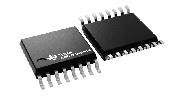
The CD4504B types are supplied in 16-lead hermetic dual-in-line ceramic packages (F3A suffix), 16-lead dual-in-line plastic packages (E suffix), 16-lead small-outline packages (M, M96, and MT suffixes), and 16-lead thin shrink small-outline packages (PW and PWR suffixes).


