Catalog
Low-Power Multiple Drivers And Receivers
Key Features
• Meets or Exceeds the Requirements of TIA/EIA-232-F and ITU Recommendation V.28Single Chip With Easy Interface Between UART and Serial-Port ConnectorLess Than 9-mW Power ConsumptionWide Driver Supply Voltage...4.5 V to13.2 VDriver Output Slew Rate Limited to30 V/us MaxReceiver Input Hysteresis...1100 mV TypPush-Pull Receiver OutputsOn-Chip Receiver 1-us Noise FilterFunctionally Interchangeable With Texas Instruments SN75185Operates Up to 120 kbit/s Over a 3-Meter Cable(SeeApplication Informationfor Conditions)Meets or Exceeds the Requirements of TIA/EIA-232-F and ITU Recommendation V.28Single Chip With Easy Interface Between UART and Serial-Port ConnectorLess Than 9-mW Power ConsumptionWide Driver Supply Voltage...4.5 V to13.2 VDriver Output Slew Rate Limited to30 V/us MaxReceiver Input Hysteresis...1100 mV TypPush-Pull Receiver OutputsOn-Chip Receiver 1-us Noise FilterFunctionally Interchangeable With Texas Instruments SN75185Operates Up to 120 kbit/s Over a 3-Meter Cable(SeeApplication Informationfor Conditions)
Description
AI
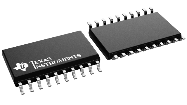
The SN75C185 is a low-power BiMOS device containing three independent drivers and five receivers that are used to interface data terminal equipment (DTE) with data circuit-terminating equipment (DCE). Typically, the SN75C185 replaces one SN75188 and two SN75189 devices. This device conforms to TIA/EIA-232-F. The drivers and receivers of the SN75C185 are similar to those of the SN75C188 and SN75C189A, respectively. The drivers have a controlled output slew rate that is limited to a maximum of 30 V/us, and the receivers have filters that reject input noise pulses that are shorter than 1 us. Both these features eliminate the need for external components.
The SN75C185 uses the low-power BiMOS technology. In most applications, the receivers contained in this device interface to single inputs of peripheral devices such as ACEs, UARTS, or microprocessors. By using sampling, such peripheral devices usually are insensitive to the transition times of the input signals. If this is not the case, or for other uses, it is recommended that the SN75C185 receiver outputs be buffered by single Schmitt input gates or single gates of the HCMOS, ALS, or 74F logic families.
The SN75C185 is characterized for operation from 0°C to 70°C.


