THS1209 Series
12 Bit, 8 MSPS ADC Dual Ch., DSP/uP Interface, Channel Autoscan, Low Power
Manufacturer: Texas Instruments
Catalog
12 Bit, 8 MSPS ADC Dual Ch., DSP/uP Interface, Channel Autoscan, Low Power
Key Features
• Simultaneous Sampling of 2 Single-Ended Signals or 1 Differential SignalSignal-to-Noise Ratio: 68 dB at fI= 2 MHzDifferential Nonlinearity Error: ±1 LSBIntegral Nonlinearity Error: ±1.5 LSBAuto-Scan Mode for 2 Inputs3-V or 5-V Digital Interface CompatibleLow Power: 218 mW Max at 5 VPower Down: 1 mW Max5-V Analog Single Supply OperationInternal Voltage References ...50 PPM/°C and ±5% AccuracyGlueless DSP InterfaceParallel µC/DSP InterfaceAPPLICATIONSRadar ApplicationsCommunicationsControl ApplicationsHigh-Speed DSP Front-EndAutomotive ApplicationsSimultaneous Sampling of 2 Single-Ended Signals or 1 Differential SignalSignal-to-Noise Ratio: 68 dB at fI= 2 MHzDifferential Nonlinearity Error: ±1 LSBIntegral Nonlinearity Error: ±1.5 LSBAuto-Scan Mode for 2 Inputs3-V or 5-V Digital Interface CompatibleLow Power: 218 mW Max at 5 VPower Down: 1 mW Max5-V Analog Single Supply OperationInternal Voltage References ...50 PPM/°C and ±5% AccuracyGlueless DSP InterfaceParallel µC/DSP InterfaceAPPLICATIONSRadar ApplicationsCommunicationsControl ApplicationsHigh-Speed DSP Front-EndAutomotive Applications
Description
AI
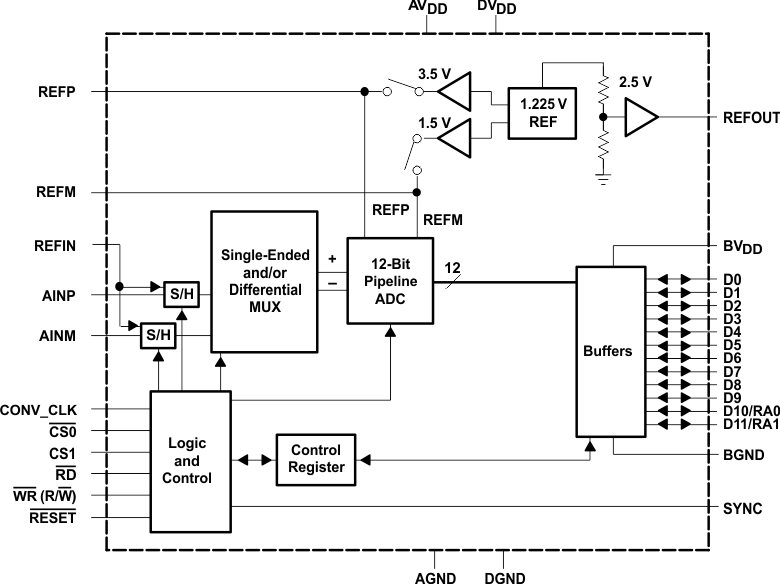
The THS1209 is a CMOS, low-power, 12-bit, 8 MSPS analog-to-digital converter (ADC). The speed, resolution, bandwidth, and single-supply operation are suited for applications in radar, imaging, high-speed acquisition, and communications. A multistage pipelined architecture with output error correction logic provides for no missing codes over the full operating temperature range. Internal control registers allow for programming the ADC into the desired mode. The THS1209 consists of two analog inputs, which are sampled simultaneously. These inputs can be selected individually and configured to single-ended or differential inputs. Internal reference voltages for the ADC (1.5 V and 3.5 V) are provided. An external reference can also be chosen to suit the dc accuracy and temperature drift requirements of the application.
The THS1209C is characterized for operation from 0°C to 70°C, and the THS1209I is characterized for operation from –40°C to 85°C.


